1. Introduction
The XCZU9EG core board uses the Xilinx Zynq UltraScale+ MPSoCs EG series FPGA as the main control chip, model XCZU9EG-2FFVB1156I. The physical image of the core board is shown in Figure 1.1:
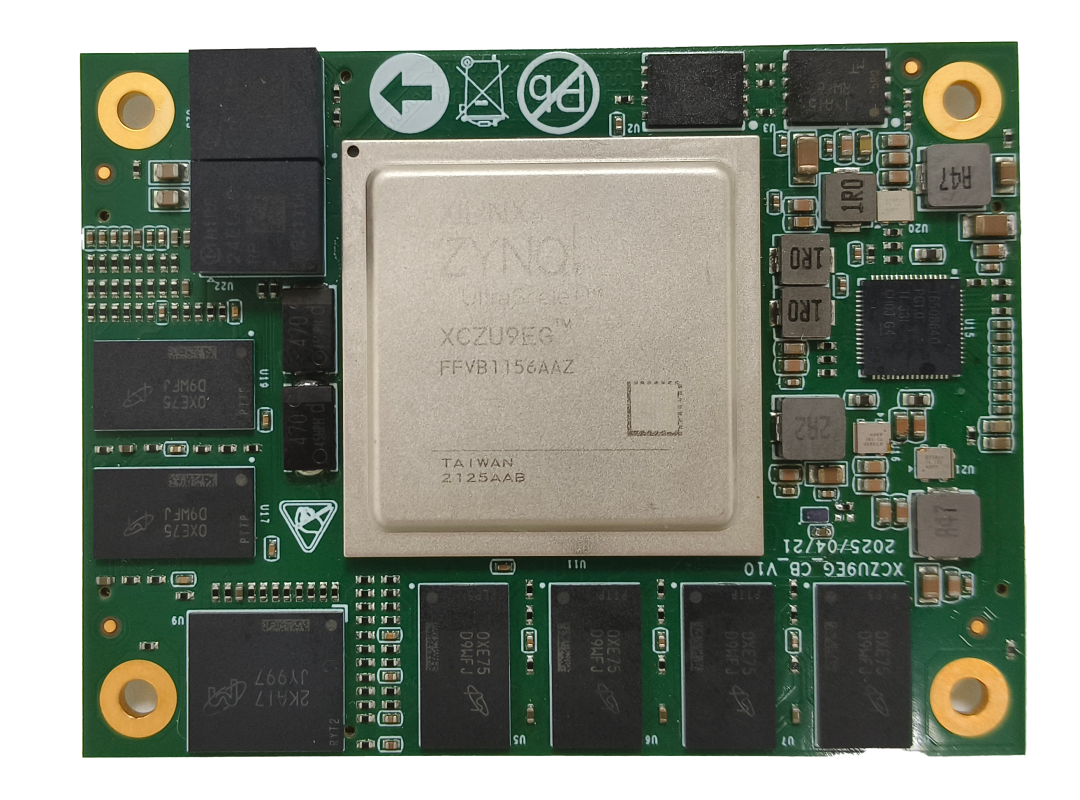
Figure 1.1 Physical image of the XCZU9EG core board
This core board integrates 6 Micron DDR4 chips (model: MT40A512M16LY-062E), with 4 chips mounted on the PS side, forming a 64-bit data bus bandwidth and 4GB capacity; 2 chips mounted on the PL side, forming a 32-bit data bus bandwidth and 2GB capacity. The maximum operating data rate supported by the DDR4 SDRAM on the PS and PL sides is 2400Mbps. Additionally, the core board integrates 2 pieces of 256Mb QSPI Flash and 1 piece of 8GB eMMC Flash chip, used for boot configuration storage and system file storage, respectively.
The core board is resource-rich, with abundant chip interfaces, facilitating secondary development.
The structural diagram of the XCZU9EG core board is shown in Figure 1.2:
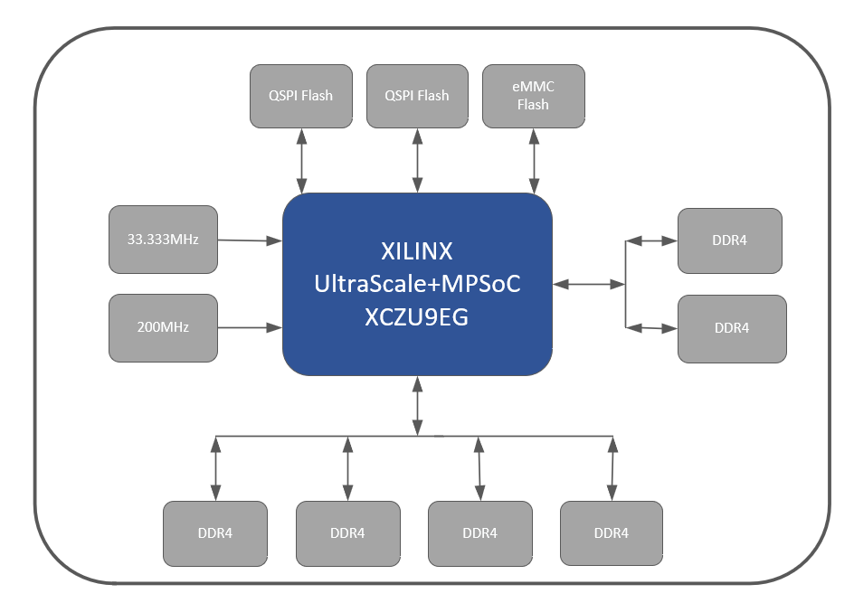
Figure 1.2 Structural diagram of the XCZU9EG core board
2. Power Supply
The power supply voltage for the XCZU9EG core board is +12V, supplied through connector J10. The core power of the XCZU9EG is achieved by paralleling 2 MYMGM1R824ELA5RP power chips, with a maximum current of 50A. Additionally, a PMIC chip designed specifically for Xilinx Zynq multiprocessor system-on-chip (MPSoC) and field-programmable gate array (FPGA) series is used to generate all other power supplies required by the XCZU9EG chip, model TPS6508640.
The overall framework of TPS6508640 is shown in Figure 2.1:
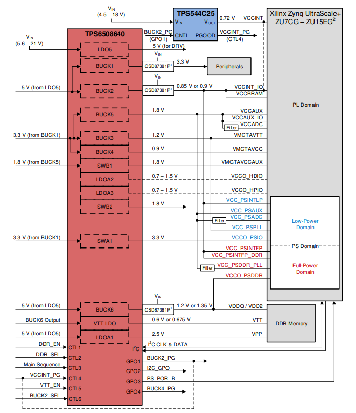
Figure 2.1 Overall framework of TPS6508640
3. ZYNQ Chip
This core board is equipped with the Xilinx Zynq UltraScale+ MPSoC EG series chip XCZU9EG-2FFVB1156I.
The overall block diagram of this chip is shown in Figure 3.1:
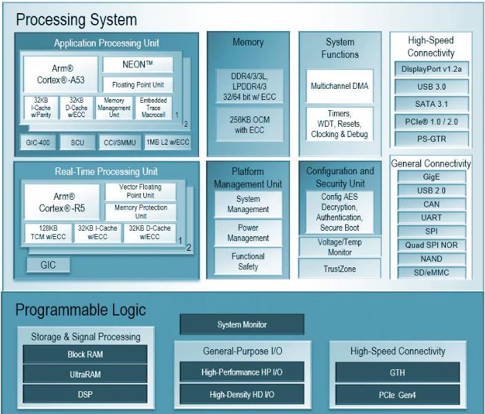
Figure 3.1 Overall framework of XCZU9EG-2FFVB1156I
This chip has the following features:
Processing System (PS):
Integrates 4 ARM Cortex™-A53 processors, with a maximum frequency of 1.3GHz, supporting secondary cache. Integrates 2 Cortex-R5 processors, with a maximum frequency of 533MHz.
Supports various memory interfaces:
32/64 bit DDR4, LPDDR4, DDR3, DDR3L, LPDDR3.
Provides rich high-speed peripheral interfaces:
PCIe Gen2, USB 3.0, SATA 3.1, DisplayPort.
Integrates common peripheral interfaces:
USB 2.0, Gigabit Ethernet, SD/SDIO, I2C, CAN, UART, GPIO.
Programmable Logic (PL):
Includes abundant programmable logic units, DSP Slices, and block RAM (BRAM) resources.
The parameters of each module of this chip are as follows:
1. Main parameters of the PS system:
Processor Cores:
ARM Quad-core Cortex™-A53: Maximum frequency of 1.3GHz; each core is equipped with 32KB L1 instruction cache and 32KB L1 data cache; 1MB L2 cache (shared among four cores).
ARM Dual-core Cortex-R5: Maximum frequency of 533MHz; each core is equipped with 32KB L1 instruction cache and 32KB L1 data cache; each core integrates 128KB tightly coupled memory (TCM).
Memory Interfaces:
External Memory: Supports 32/64 bit DDR4, DDR3, DDR3L, LPDDR4, LPDDR3.
Static Memory: Supports NAND Flash and 2 Quad-SPI Flash.
High-Speed Interfaces:
Supports PCIe Gen2 x4, 2x USB 3.0, SATA 3.1, DisplayPort, 4x Tri-mode Gigabit Ethernet.
General Interfaces:
Supports 2x USB 2.0, 2x SD/SDIO, 2x UART, 2x CAN 2.0B, 2x I2C, 2x SPI, 4x 32-bit GPIO.
Power Management:
Supports Full (full power domain), Low (low power domain), PL (programmable logic domain), Battery (battery domain) power management.
Encryption Engine:
Supports RSA, AES, SHA encryption algorithms.
System Monitoring:
Integrates a 10-bit 1Msps ADC for on-chip temperature and voltage monitoring.
PL Logic Main Parameters:
System Logic Cells: 600K
CLB Flip-Flops: 548K
CLB LUTs: 274K
Block RAM: 32.1 Mb (approximately 4.01 MB)
Clock Management Units (CMTs): 4
DSP Slices: 2520
High-Speed Transceivers: 24 GTH transceivers, with rates up to 16.3 Gb/s
Chip Specifications:
Model: XCZU9EG-2FFVB1156I
Speed Grade: -2
Temperature Grade: Industrial (I)
Package: FFVB1156
4. DDR4 DRAM
The XCZU9EG core board is equipped with 6 Micron (Micron) DDR4 SDRAM chips, model MT40A512M16LY-062E (single chip capacity 8Gb). Its configuration is as follows:
PS Side Storage Subsystem:
Mounted Chips: 4
Bus Width: 64 bits
Total Capacity: 4GB
Maximum Operating Speed: 1200MHz
Connection Method: Directly connected to the memory interface of PS Bank 504.
PL Side Storage Subsystem:
Mounted Chips: 2
Bus Width: 32 bits
Total Capacity: 2GB
Maximum Operating Speed: 1200MHz (corresponding data rate 2400 Mbps)
Connection Method: Connected to the interfaces of FPGA Bank 64 and Bank 65.
5. QSPI FLASH
The XCZU9EG core board integrates 2 Micron (Micron) Quad-SPI Flash chips, model MT25QU256ABB1EW9 (single chip capacity 256Mb). The two Flash chips work in parallel, forming an 8-bit data bus and using 1.8V CMOS level standards.
With its non-volatile storage characteristics, this QSPI Flash array can be used as the system’s boot device, storing the following critical images:
○ FPGA bitstream (bit file)
○ ARM application code
○ Other user data files
This QSPI Flash array is connected to the dedicated interface pins of PS Bank 500 of the Zynq UltraScale+ chip. During system design, the corresponding PS MIO pins on Bank 500 need to be configured for Quad-SPI Flash interface functionality.
6. eMMC FLASH
The XCZU9EG core board integrates 1 piece of 8GB eMMC Flash chip, model MTFC8GAKAJCN-4MIT.
○ Interface Standard: Complies with JEDEC e-MMC V5.0 standard, using HS-MMC interface.
○ Level Support: 1.8V or 3.3V.
○ Connection Method: Connected to the Zynq UltraScale+ chip via an 8-bit data bus.
With its large capacity and non-volatile characteristics, this eMMC Flash can serve as a large-capacity storage device in the system, used for storing:
○ ARM applications
○ System files
○ Other user data files
7. Clock Configuration
This core board provides independent reference clocks and RTC real-time clocks for the PS system and PL logic, supporting independent operation of both.
○ PS System RTC Real-Time Clock:
Provided by the passive crystal X2 on the core board, offering a 32.768 kHz clock source.
Connected to the dedicated pins of Zynq UltraScale+ chip PS Bank 503: PS_PADI_503_V21 and PS_PADO_503_V22.
○ PS System Reference Clock:
Provided by the crystal oscillator X1 on the core board, offering a 33.333 MHz clock input.
Connected to the pins of Zynq UltraScale+ chip PS Bank 503: PS_REF_CLK_503_U24.
○ PL System Reference Clock:
Provided by the differential oscillator on the core board, offering a 200 MHz clock source.
Mainly used as the reference clock for the PL side DDR4 controller.
The output is connected to the global clock input pin of PL Bank 64.
This global clock can be used to drive the DDR4 controller on the PL side and user-defined logic circuits.
8. Connectors
The XCZU9EG core board has a total of 4 high-speed expansion ports (J9-J12), using 4 120-pin board-to-board connectors, with connector model AXK5A2137YG, and the connector model used on the baseboard is AXK6A2337YG.

Share💬 Like👍 View❤️ Support with a “triple click”!