Click the “Computer Vision Life” above and select “Star”.
Quickly obtain the latest insights.

 1. Introduction
The intelligence of autonomous vehicles depends on algorithms, leading to the emergence and popularity of the concept of software-defined vehicles. However, to realize software-defined vehicles, a hardware computing platform or domain controller capable of supporting highly intelligent and computationally intensive AI algorithms is essential, and both hardware computing platforms and domain controllers rely heavily on chips. As autonomous driving progresses from L0 to L5, the enhancement of functions and performance brings better intelligence and technological experiences, while also placing higher demands on the computing power and performance of AI chips.
Previous documents have mentioned that L2 or ADAS requires AI computing power <10 TOPS, L3 requires 30~60 TOPS, L4 requires >100 TOPS, and L5 requires 500-1000 TOPS.
For domain controllers, the hardware can be roughly divided into three parts: AI processing chips that handle environmental perception and deep learning with ultra-large computing power demands, CPUs responsible for control decisions and logical operations, and MCUs responsible for functional safety and vehicle control.
The first part is usually a GPU or TPU, which handles large-scale floating-point parallel computing demands, primarily used for environmental perception and information fusion, such as the GPU unit of Xavier, Ascend 310, Horizon BPU, etc.
The second part is mostly ARM architecture, similar to a CPU, mainly responsible for logical operations and decision control, processing high-precision floating-point serial calculations.
The third part mainly ensures reliability and vehicle control, with Infineon’s TC297 or TC397 being the most commonly used currently.
Most domain controllers or computing platforms currently choose Infineon’s TriCore series TC397 or TC297 for the third part, such as Huawei, Horizon, Desay SV, and YouControl. The second part is mostly ARM architecture processors, or integrated with the first part’s AI computing module into a single SoC. The first part is currently at the forefront of industry transformation and technological exploration, and a dedicated article has been organized discussing various xPUs referred to as AI chips.
This article reviews the types and manufacturers of AI chips currently available for designing domain controllers or computing platforms, although the highest-performing chips can only meet the needs of some L3 and L4 level autonomous driving AI calculations.
2. Overview of Autonomous Driving AI Chips
1. Huawei MDC and Ascend Chips
Huawei launched the MDC intelligent driving computing platform and high-level autonomous driving full-stack solution in 2018, including two platforms, MDC300 and MDC600, corresponding to L3 and L4 level autonomous driving, respectively.
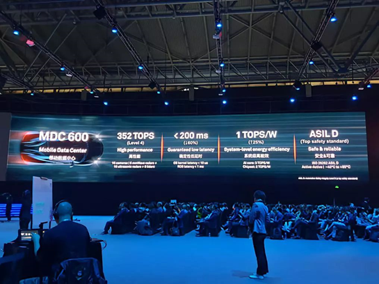
The Huawei MDC300 consists of the Huawei Ascend310 chip, Huawei Kunpeng chip, and Infineon’s TC397, with a computing power of around 64 TOPS, meeting the L3 level autonomous driving computing power requirements. The MDC600 is based on eight Ascend 310 AI chips and integrates a CPU and corresponding ISP modules, achieving a computing power of up to 352 TOPS.
Compared to other platforms, the biggest advantage of Huawei MDC is its unified system architecture, which facilitates functional expansion and adaptation to various application scenarios. Moreover, the Huawei MDC intelligent driving computing platform passed the ISO26262 functional safety management certification issued by TÜV Rheinland on January 16, 2020, reaching the ASIL-D level standard.
Leveraging its experience in the ICT industry, Huawei has established a complete chip system, including the Balong series chips dedicated to supporting 5G, the Ascend series AI chips developed based on the new Da Vinci architecture, the Kirin series CPU processors used in mobile phones, and the Kunpeng series server-grade processor chips. Among these, the Ascend series AI chips are focused on AI computing needs.
The Ascend 310 uses Huawei’s self-developed efficient and flexible CISC instruction set, with each AI core capable of completing 4096 MAC calculations in one cycle, integrating various computing units such as tensor, vector, and scalar, supporting multiple mixed-precision calculations, and supporting data precision calculations for both training and inference scenarios.
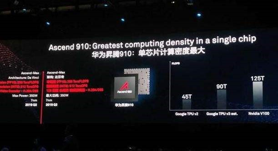
As an NPU, the Ascend 310 integrates the advantages of both FPGA and ASIC chips, including the low power consumption of ASIC and the programmability and high flexibility of FPGA, allowing its unified architecture to adapt to various scenarios, with power consumption ranging from tens of milliwatts to hundreds of watts, and elastic multi-core stacking, providing optimal energy consumption ratios in various scenarios.
In comparison, NVIDIA’s Xavier has a computing power of 30 TOPS and a power consumption of 30W, with an energy efficiency of 1 TOPS/W. In contrast, Huawei’s Ascend 310 has a computing power of 16 TOPS and a power consumption of only 8W, achieving an energy efficiency of 2 TOPS/W.
The Huawei self-developed Ascend chip supports the access and real-time processing of more external sensor data streams (such as cameras, millimeter-wave radar, lidar, GPS, etc.), providing safer and more reliable computing power support for autonomous driving, capable of handling more complex road conditions. The MDC equipped with Ascend chips has high performance, energy efficiency, safety, and deterministic low latency advantages compared to other computing platforms.
2. Huawei HiSilicon Kirin Chips
Speaking of Huawei, it is worth mentioning HiSilicon, established in 2004, and the renowned Kirin series chips.
The first SoC launched by HiSilicon was Kirin 910, which, as a smart mobile SoC, includes important modules such as baseband, graphics processing unit (GPU), digital signal processor (DSP), and image signal processor (ISP), in addition to the CPU.
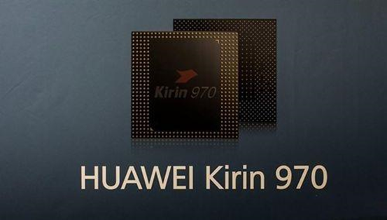
In September 2017, Huawei officially launched its new AI chip “Kirin 970” at the IFA in Berlin, Germany. The Kirin 970 uses TSMC’s 10nm process, integrates 5.5 billion transistors, reduces power consumption by 20%, and achieves a peak download rate of 1.2Gbps. The Kirin 970 is built on the Cambricon NPU architecture, innovatively designed with the HiAI mobile computing architecture, significantly outperforming CPU and GPU in AI performance density. Compared to four Cortex-A73 cores, the Kirin 970 has about 50 times the energy efficiency and 25 times the performance advantage for the same AI tasks. Huawei HiSilicon has successively launched Kirin 980/985/990 and other series SoCs, all optimized for AI computing.
Recently, it has been reported that Huawei has signed a cooperation agreement with BYD, and future BYD new cars will use Huawei’s Kirin chips.
However, surprisingly, the first chip used in vehicles by Huawei is not the mature Kirin 970 or the latest 990, but the older Kirin 710A chip. The Kirin 710 chip was released in July 2018, featuring an 8-core design that includes four A73 large cores and four A53 small cores, with a large core frequency of 2.2GHz; the Kirin 710A, positioned lower and with older cores, is developed from the Kirin 710, maintaining the same architecture and cores, but the process has shifted from 12nm to 14nm, with the large core frequency reduced to 2.0GHz.
Why choose the outdated Kirin 710A chip with a backward process level for vehicle use?
We know that due to various measures taken by the US against Huawei, Huawei’s supplier channels have been severely affected, especially in chip foundry, as TSMC is no longer reliable, and Huawei’s chips can only turn to domestic foundries, with the only capable one being SMIC. However, SMIC’s process can only reach 14nm, making it impossible to handle the 7nm Kirin 970 and other chips; after much consideration, the Kirin 710A became the most suitable option.
From an application demand perspective, the current Kirin 710A can meet the functional performance requirements of current smart vehicle systems, mainly in image and audio processing, as well as interaction smoothness. Its competitors, such as Intel Atom A3950 and Qualcomm Snapdragon 820A chips, have already begun mass production in vehicles, such as Li Xiang ONE, Lynk & Co 05, and Xpeng P7. However, the Kirin 710A needs to pass vehicle-grade certification before formal mass production.
3. Horizon Robotics Journey Chips
Horizon Robotics was founded in July 2015 by Yu Kai, former vice president of Baidu Research Institute and director of Baidu Deep Learning Lab, dedicated to providing complete embedded AI solutions (robot brains) for B-end users involving both algorithms and hardware.
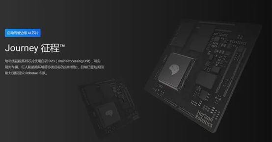
In December 2017, Horizon released China’s first globally leading embedded AI chip—the Journey 1.0 processor for intelligent driving and the Sunrise 1.0 processor for intelligent cameras, along with AI solutions targeting intelligent driving, smart cities, and intelligent business.
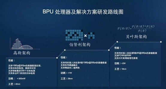
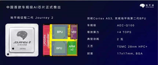
In August 2019, Horizon announced the mass production of China’s first vehicle-grade AI chip—Journey 2. The Journey 2 chip is equipped with Horizon’s independently developed high-performance computing architecture BPU2.0 (Brain Processing Unit), using TSMC’s 28nm process technology, achieving more than 10 times the performance of equivalent GPUs in terms of computing power per TOPS, with visual perception capable of achieving recognition accuracy >99% and latency <100 milliseconds. Journey 2 is mainly aimed at ADAS market perception solutions, providing more than 4 TOPS of equivalent computing power, primarily used for detecting vehicles, pedestrians, and road environments in autonomous driving, similar to Mobileye Q series chips.
At CES 2020, Horizon released the Matrix 2 platform based on its self-developed Journey 2 chip, achieving a computing power of 16 TOPS. At the same time, Horizon plans to launch Journey 5 by the end of 2020, with a computing power of 96 TOPS and a power consumption of 15W, supporting 16 camera inputs, targeting Tesla FSD.
Based on its self-developed computing platform and product matrix, Horizon has supported solutions for different levels of autonomous driving such as L2, L3, and L4. In the intelligent driving field, Horizon’s business connections with the four major automotive markets (the US, Germany, Japan, and China) continue to deepen, currently empowering partners including Audi, Bosch, Changan, BYD, SAIC, and GAC among top-tier Tier 1 and OEM manufacturers domestically and abroad.
4. Cambricon-1M/MLU100
Cambricon Technologies was founded in March 2016, originally a research group under the Institute of Computing Technology, Chinese Academy of Sciences, and is one of the earliest chip companies to enter the AI computing field. Its main focus is on high-performance server chips, high-performance terminal chips, and service robot chips, but Cambricon emphasizes the artificial intelligence field. As early as 2016, it launched its first commercial deep learning processor, Cambricon 1A. In 2018, Cambricon released several IP products—terminal chips Cambricon-1M using 7nm technology, and cloud-based smart chips MLU100.
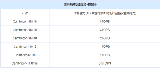
The Cambricon-1M processor IP is a third-generation product, primarily targeting the intelligent driving field, later expanding its application areas to smartphones, smart speakers, cameras, and autonomous driving. The Cambricon-1M’s int 8 (8-bit operation) performance reaches 5 TOPS/W (50 trillion operations per watt), and it provides three sizes of processing cores: 2 TOPS, 4 TOPS, and 8 TOPS to meet different needs. The 1M also supports CNN, RNN, SVM, k-NN, and various deep learning models and machine learning algorithms, capable of completing tasks such as vision, speech, and natural language processing. By flexibly configuring the 1M processor, it maximizes resource utilization for multi-threaded and complex autonomous driving tasks. It also supports terminal training to avoid sensitive data transmission and achieve faster responses.
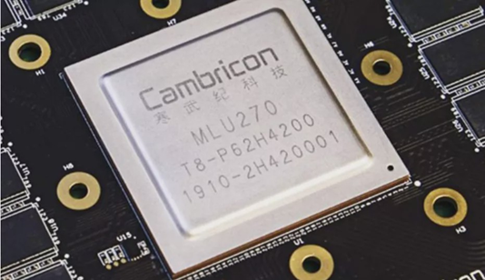
The first cloud-based intelligent chip Cambricon MLU100 adopts Cambricon’s latest MLU V01 architecture and TSMC’s 16nm process, capable of operating in balanced mode (1GHz frequency) and high-performance mode (1.3GHz frequency), achieving equivalent theoretical peak speeds of 128 trillion fixed-point operations and 166.4 trillion fixed-point operations, with a power consumption of 80W and 110W, respectively. The MLU100 cloud chip also has high universality, supporting various deep learning and commonly used machine learning algorithms.
5. Baidu Kunlun AI Chip
On July 4, 2018, Baidu released its first AI chip—Kunlun—at its developer conference. Baidu introduced Kunlun as China’s first cloud-based full-featured AI chip, based on Baidu’s CPU, GPU, and FPGA accelerators, developed through eight years of research and over 20 iterations. The design performance exceeds 100W power consumption, providing 260 TOPS computing power, with a memory bandwidth of 512GB/s and thousands of cores. It is said that the Kunlun chip will be manufactured by Samsung using a 14nm process.
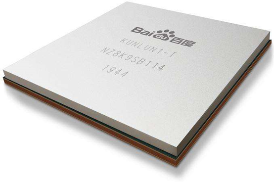
On December 18, 2019, Samsung officially announced that Baidu’s first AI chip Kunlun had completed development and would be mass-produced as early as early 2020. This Baidu self-developed SoC aimed at cloud, edge, and AI is currently the highest-performing SoC.
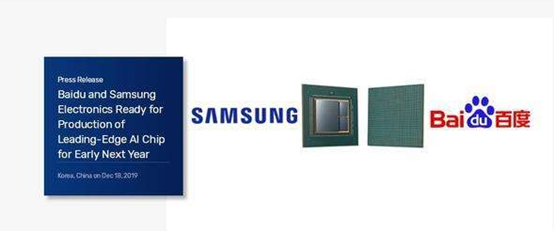
The Kunlun chip adopts the I-Cube packaging solution, connecting logic chips and high-bandwidth memory with insert technology, utilizing Samsung’s differentiated solutions to provide higher density/bandwidth at the smallest size.
In terms of computing power, the Kunlun chip offers a memory bandwidth of 512 GBps, achieving 260 TOPS of computing power at 150W power consumption; it supports pre-trained models for natural language processing Ernie, with an inference speed three times faster than traditional GPU/FPGA accelerated models.
With Kunlun, Baidu can support various functions, including large-scale AI computing, such as search ranking, speech recognition, image processing, natural language processing, autonomous driving, and deep learning platforms like PaddlePaddle.
6. SemiDrive 9 Series SoC
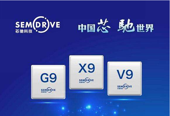
On May 28, Nanjing SemiDrive Semiconductor Technology Co., Ltd. officially released its 9 series X9, V9, and G9 automotive chip products, providing a coordinated integrated solution for smart cabins, intelligent driving, and central gateways.
According to SemiDrive, the X9, V9, and G9 are all domain control-level large SOC chips, with a single chip capable of replacing multiple traditional ECUs, supporting multiple in-vehicle operating systems such as QNX, Linux, and Android, and also supporting AutoSAR to meet customer needs for flexible adaptation.
The X9 series chip is used to support future intelligent cabins: the X9 features Imagination’s PowerVR Series9XM graphics processor (GPU), with a single X9 chip capable of supporting multiple high-definition screens, featuring voice interaction, gesture recognition, and driver status monitoring.
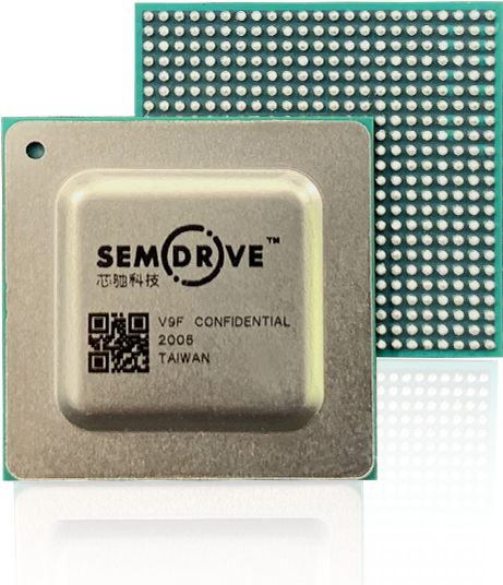
The V9 series chip is defined as the core brain for autonomous driving, serving as the core of the domain controller. The V9 includes a high-performance vision engine, supporting up to 18 camera inputs, not only meeting the needs of ADAS applications but also leaving ample expansion space for more advanced autonomous driving and unmanned driving in the future.
The G9 series chip serves as the smart information hub for future vehicles, facilitating interaction and connectivity for intelligent cabins, domain controllers, and other modules, while also connecting to external networks and supporting OTA online upgrades.
The V9 series processor integrates the latest high-performance engines, including 64-bit Arm® Cortex®-A55 cores, V8.2 architecture CPU; high-performance PowerVR GPU; CV-specific vision processing engine, meeting the growing demand for strong computing power in next-generation intelligent driving assistance systems. Additionally, the V9 series processor integrates Gigabit Ethernet, CAN-FD, allowing seamless connection with in-vehicle systems at lower costs. This processor also supports MIPI-CSI and parallel CSI, accommodating camera inputs, including 360° surround imaging systems, front-facing cameras, rear-facing cameras, and in-car cameras.
Imagination, located in the UK, provides GPU support for SemiDrive, with the latest generation neural network accelerator (NNA) PowerVR Series3NX offering up to 160 TOPS of computing power for SemiDrive’s autonomous driving chips; for its high-end cabin chips, Imagination’s latest IMG A series (IMG A-Series) GPU provides higher performance, faster processing speeds, and lower power consumption.
Additionally, SemiDrive claims to be the first company in China to obtain TÜV Rheinland’s ISO 26262:2018 functional safety management system certification.
7. Black Sesame Huashan No. 2
On the evening of June 15, 2020, Black Sesame Technology released its self-developed vehicle-grade chip, the Huashan No. 2 A1000 and A1000L, which is the second generation product following Huashan No. 1. Both chips use TSMC’s 16nm process, supporting automotive-grade AEC-Q100 standards and multiple sensors.
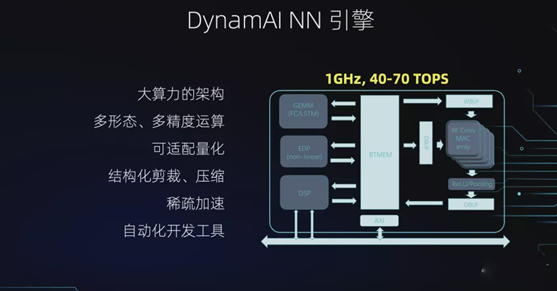
The Huashan No. 2 A1000 competes with Tesla, featuring eight CPU cores and providing 40 TOPS of computing power with a power consumption of 8-10W. According to Black Sesame Intelligent Technology, the A1000 is the world’s top high-performance vehicle-grade SOC chip that includes functional safety, and it is currently the first mass-producible vehicle-grade chip in China that meets the requirements for L3/L4 level autonomous driving. The Huashan No. 2 A1000 is positioned against Tesla at the L3 level, with its power consumption only a quarter of that of Tesla’s FSD, an area only one-third, and a cost also only a quarter, making it a cost-effective product. By the end of 2021, models equipped with Black Sesame Huashan No. 2 chips are expected to enter mass production.
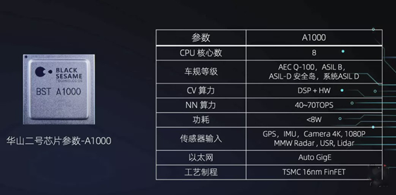
In comparison, Tesla’s FSD has a computing power of 144 TOPS and a power consumption of 72W, with an energy efficiency ratio of 2 TOPS/W; NVIDIA’s Xavier has a computing power of 30 TOPS and a power consumption of 30W, with an energy efficiency ratio of 1 TOPS/W. The Huashan No. 2 A1000 single chip achieves an energy efficiency ratio exceeding 6 TOPS/W, and the domain controller formed by two chips interconnected achieves an energy efficiency ratio exceeding 5 TOPS/W.
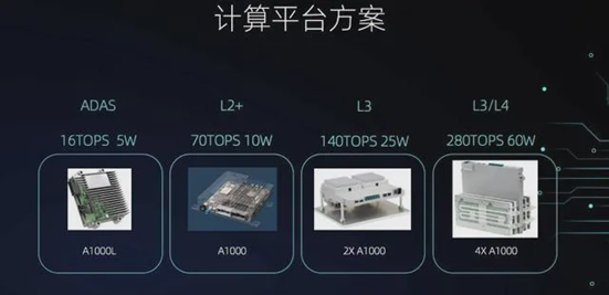
According to the computing platform scheme provided by Black Sesame, a single A1000L chip is suitable for low-level ADAS assisted driving; a single A1000 chip is suitable for L2+ autonomous driving; a domain controller composed of interconnected dual A1000 chips can support L3 level autonomous driving; and four A1000 chips stacked can be used for future L4 level autonomous driving.
8. Westwell Brain-like Chips
Westwell Technology was founded in 2015 and initially focused on brain-like chips. Brain-like chips are designed and manufactured based on the working principles of the human brain.
Brain-like chips mimic the working form of brain neurons, differing from von Neumann architecture processor chips, where the processing units are neurons and memory is synapses. Neurons and synapses are physically connected, so each neuron calculation is local, while globally, neurons work in a distributed manner. Due to their characteristics of local computation and distributed work, brain-like chips have advantages in work efficiency and energy consumption compared to von Neumann architecture processor chips.
Westwell initially developed the “DeepSouth” brain-like chip, which is the world’s first commercially available chip simulating 50 million brain-like “neurons,” while IBM’s “TrueNorth” at the same time could only simulate 1 million.
Based on brain-like chip technology, Westwell developed two AI chips, “DeepWell” and “VestWell,” with DeepWell peak performance of 1.8 TOPS, single-core power consumption of 500mW, and dual-core power consumption of 1W; VestWell chip peak performance of 4 TOPS, with power consumption of less than 2W.

Compared to products like NVIDIA Xavier and Horizon Journey 2 with dozens of TOPS of computing power, Westwell’s two chips seem somewhat lacking. However, these two chips can achieve on-chip learning, allowing for the addition of new samples for incremental training to improve inference accuracy.
Currently, autonomous driving algorithms are trained using high-performance servers, and the trained models are then deployed onto in-vehicle hardware. The advantage of Westwell’s chips is that they can evolve autonomously; specifically, the on-chip learning feature of Westwell’s AI chips enables localization of the model training process, meaning machine learning can be completed directly on the terminal chip, continuously improving computational judgment accuracy through ongoing learning and refinement, allowing for self-evolution. Compared to other chips with OTA upgrades, Westwell’s chips offer a shortcut.
9. DeepVision Technology DPU
DeepVision Technology was founded by a Tsinghua team in 2016, and its products are called “Deep Processing Units” (DPU), aimed at achieving performance superior to GPUs with ASIC-level power consumption. Currently, the first batch of products is based on the FPGA platform. On July 17, 2018, DeepVision Technology was acquired by Xilinx, the world’s largest FPGA manufacturer.
DeepVision aims to create an end-to-end deep learning hardware solution based on DPU, which includes not only the DPU chip architecture on hardware modules (customized PCB boards) but also a DPU compression compilation toolchain SDK tailored for this architecture.
Since its establishment in 2016, DeepVision has been developing machine learning solutions based on Xilinx’s technology platform, launching two underlying architectures for deep learning processors—the Aristotle architecture and the Cartesian architecture based on Xilinx FPGA devices.
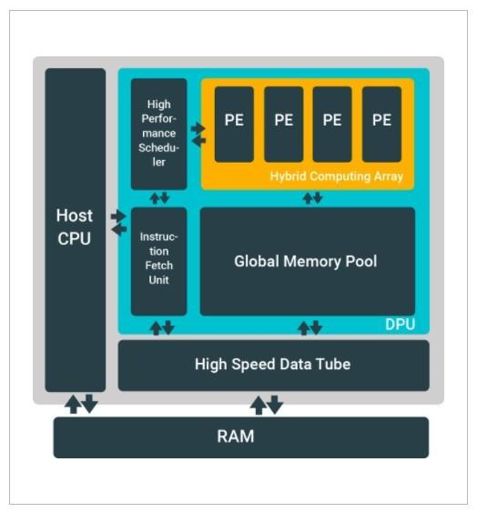
Aristotle Architecture
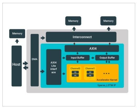
Cartesian Architecture
Based on the above two hardware architectures, DeepVision has also released several DPU hardware products. In facial recognition, DeepVision has launched the DP-1200-F01 facial detection and recognition module and the DP-2100-F16 facial analysis solution. Subsequently, DeepVision launched the video structuring solution DP-2100-O16, capable of real-time structuring of 16 channels of 1080p HD video, detecting, tracking, and analyzing attributes of people, vehicles, and non-motor vehicles.
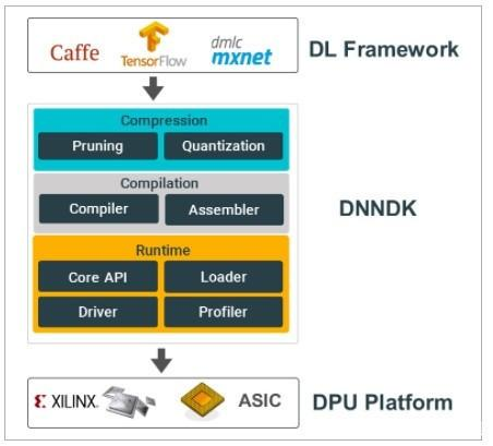
On top of the hardware, DeepVision has developed a deep neural network development kit (DNNDK) tailored for the aforementioned DPU, which is also the first SDK developed specifically for deep learning in China.
10. XILINX SoC MP SoC
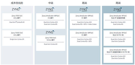
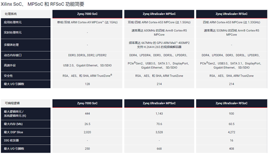
Xilinx is a pioneer and leader in FPGA technology, having created many industry firsts, such as the world’s first FPGA, the first hardware/software programmable SoC, the first multi-processor SoC (MPSoC, integrating ARM CPU cores and Mali series GPUs on an FPGA), and the first RFSoC (integrating communication-grade RF sampling data converters, SD-FEC cores, ARM processors, and FPGA architecture into a single chip device).
In July 2018, Xilinx’s acquisition of DeepVision Technology was seen as a move to further strengthen its layout in the ADAS/autonomous driving market.
In automotive ADAS and autonomous driving solutions, Xilinx offers the Zynq UltraScale+ MPSoC for autonomous driving central controllers, Zynq-7000/Zynq UltraScale+ MPSoC for in-vehicle front cameras, and Zynq UltraScale+ MPSoC for multi-sensor fusion systems.
In November 2019, Xilinx announced the launch of two 16nm automotive-grade chips, Zynq UltraScale+ MPSoC 7EV and 11EG, supporting L2 to L4 level autonomous driving systems. The MPSoC integrates a 64-bit quad-core ARM Cortex A53 and dual-core ARM Cortex-R5 high-performance processors, along with Xilinx’s UltraScale architecture. So far, the XA series MPSoC has been widely used by 29 automotive brands, including Daimler-Benz, along with top-tier component suppliers such as Aptiv, Autoliv, Bosch, and Continental.
11. Tesla FSD Chip
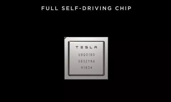
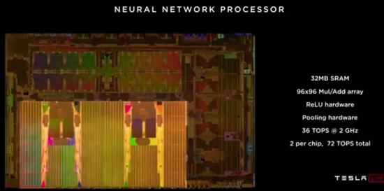
Tesla is a unique presence in the automotive industry, capable of handling cars, rockets, chips, and more, and doing it well. Initially, Tesla collaborated with chip suppliers and focused on vehicle production, but after realizing that chip suppliers were unreliable, it “abandoned” Mobileye and NVIDIA, starting its own AI chip development. In April 2019, Tesla released its first autonomous driving chip, FSD (Full Self Driving), launched directly in mass production, which Musk called “the best chip in the world.” This chip, in addition to conventional CPUs and GPUs, is equipped with two neural network processors (NNP), achieving 144 TOPS of computing power and 72W of power consumption, with an energy efficiency ratio of 2 TOPS/W, currently regarded as the best autonomous driving chip in mass production.
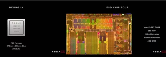
The FSD chip is manufactured using a 14nm FinFET CMOS process, measuring 260mm, with 6 billion transistors and 250 million logic gates. FSD features two neural network accelerators NNP, supporting both 32-bit and 64-bit floating-point operations, along with several ARM A72 64-bit CPUs operating at a clock frequency of 2.2 GHz, achieving 2.5 times the performance of the previous generation.
Additionally, FSD includes a safety chip to ensure that the system only runs code encrypted by Tesla and a dedicated H.265 video encoder.
Compared to the previous generation hardware, FSD’s power consumption has been reduced by approximately 1.25 times, with overall costs decreasing by 80%. Musk stated that FSD consumes about 250W per mile.
The most critical part of the self-developed FSD chip is the Neural Network Processor, with each chip containing two NNPs, each having a 96×96 MAC matrix, 32MB SRAM, operating at a frequency of 2GHz. Therefore, the processing capacity of a single NNP is 96x96x2(OPs)x2(GHz)= 36.864 TOPS, leading to a single chip computing power of 72 TOPS and an FSD hardware board computing power of 144 TOPS.
12. NVIDIA Xavier & Orin & A100
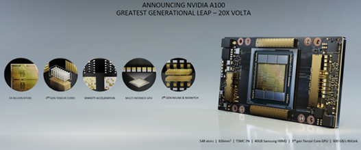
NVIDIA’s GTC 2020 was held in Huang’s kitchen due to the pandemic, where NVIDIA released its eighth-generation architecture Ampere and the first GPU based on Ampere architecture, A100. The A100 is currently the largest 7nm chip in the world, with 54 billion transistors, 3D stacking technology, and a chip area of up to 826 square millimeters, supporting TF32 and BF16 formats, featuring 438 third-generation Tensor Cores, and allowing virtual conversion into 77 GPUs to perform different tasks. Its computing power reaches 2000 TOPS, achieving a performance increase of up to 20 times compared to the Volta architecture, capable of simultaneously meeting AI training and inference needs.
In December 2019, NVIDIA launched the next-generation SOC Orin aimed at ADAS and autonomous driving, featuring 17 billion transistors, with the next-generation GPU based on the Ampere architecture and Arm Hercules CPU cores, providing 200 TOPS of computing power, seven times that of the previous generation Xavier SOC, with a power consumption of 45W, expected to be delivered in 2022, targeting L2+ level autonomous driving scenarios.
NVIDIA launched the Xavier platform at CES 2018, claiming to be the “world’s most powerful SoC”; currently, Xavier is indeed the absolute choice in the autonomous driving AI chip field, capable of processing L5 level autonomous driving data from vehicle radar, cameras, lidar, and ultrasonic systems, making it the most widely used AI chip in autonomous driving applications and one of the first to enter mass production.
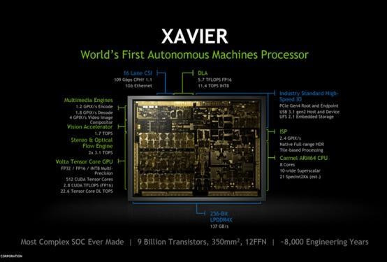
The Xavier SoC is based on TSMC’s 12nm process, integrating 9 billion transistors, with a chip area of 350 square millimeters. The CPU adopts NVIDIA’s self-developed 8-core ARM64 architecture (code-named Carmel), while the GPU utilizes 512 CUDA cores of Volta architecture, supporting FP32/FP16/INT8, with single-precision floating-point performance of 1.3 TFLOPS at a power consumption of 20W, and Tensor core performance of 20 TOPS, which can reach 30 TOPS when unlocked to 30W.
Xavier contains six different processors: Valta Tensor Core GPU, octa-core ARM64 CPU, dual NVDLA deep learning accelerators, image processor, vision processor, and video processor. These processors enable it to simultaneously and in real-time process dozens of algorithms for sensor processing, ranging, positioning and mapping, vision and perception, and path planning.
TÜVSÜD has confirmed that the NVIDIA Xavier system-on-chip meets ASIL C level of ISO 26262 random hardware integrity and meets the ASIL D level system processing capability requirements (the strictest functional safety standards).
13. Mobileye EyeQ Series
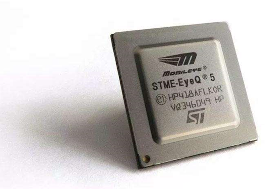
In the autonomous driving chip field, Mobileye’s EyeQ series is a typical representative of ASIC chips. As competition in the autonomous driving chip field intensifies and OEMs demand more control over AI chips, Mobileye is gradually shifting from the previous “black box” model of an integrated visual chip + algorithm supplier to an open EyeQ5 chip (allowing third-party code to run).
Mobileye is a crucial part of Intel’s layout in autonomous driving. From the perspective of processor chips, Intel’s layout is comprehensive, including Mobileye’s ADAS visual processing, Altera’s FPGA processing, as well as Intel’s Xeon processors, forming a systematic solution for the entire hardware part of autonomous driving.
The EyeQ series chips designed and developed by Mobileye are produced by STMicroelectronics. Mass-produced models range from EyeQ1 to EyeQ4, occupying about 60% of the global ADAS market share. Currently, the highest-performing EyeQ4 has a computing power of 2.5 TOPS and a power consumption of 3W, with an energy efficiency of 0.83 TOPS/W. EyeQ5 is under development and is expected to be released in 2020, targeting NVIDIA Xavier. The EyeQ5 is manufactured using 7nm FinFET technology, achieving a design computational performance of 24 TOPS, with a power consumption of 10W, making it 2.4 times more efficient than Xavier. The EyeQ5 SoC is equipped with eight multi-threaded CPU cores and will also include 18 of Mobileye’s next-generation vision processors. According to Mobileye, the EyeQ5 SoC is equipped with four heterogeneous fully programmable accelerators optimized for proprietary algorithms, including computer vision, signal processing, and machine learning. The EyeQ5 SoC also implements two PCI-E ports to support inter-processor communication. This architecture attempts to match the most suitable computing unit for each computational task, and the diversity of hardware resources allows applications to save computation time and improve computational efficiency.
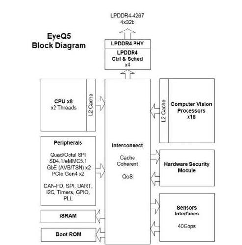
According to Mobileye’s plan, by mid-2020, a complete autonomous vehicle subsystem will be provided to partners, including a computer vision suite: a 360-degree/12 camera/300-meter range vision system and multi-chip turnkey solutions, etc.
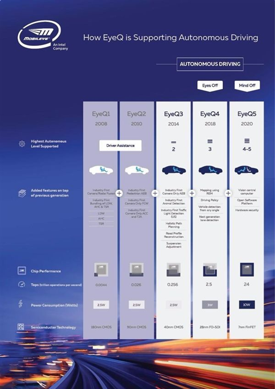
Additionally, Intel plans to combine the EyeQ5 with Atom processors to develop an AI computing platform for autonomous driving. Two EyeQ5 SoCs and one Intel Atom (凌动) processor are sufficient to achieve level 5 autonomous driving.
14. Ambarella CV2 SoC
Ambarella is a developer of high-definition imaging chips, primarily providing low-power, high-definition video compression and image processing solutions. It is dedicated to providing high-quality imaging technology at ultra-low bit rates and extremely low power consumption.
In 2018, Ambarella launched the CV2 vehicle-grade SoC, specifically designed to provide deep neural network (DNN) and stereoscopic vision processing, targeting the ADAS and autonomous driving vehicle markets, aiming to compete with Mobileye. Combining VisLab’s experience and technology, Ambarella integrated advanced computer vision, image processing, 4Kp60 video encoding, and stereoscopic vision technology into the CV2 chip, providing 20 times higher deep neural network performance than CV1.
Ambarella claims to have two competitive advantages: one is the new computer vision architecture developed by VisLab, a European computer vision and intelligent vehicle control system developer acquired by Ambarella in 2015. The second is Ambarella’s self-developed low-power, high-definition (HD) and ultra-high-definition (Ultra HD) vision processing chips.
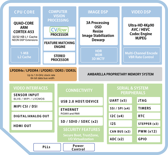
Module diagram of CV2
The CV2 chip supports four stereoscopic cameras and four monocular cameras and will be manufactured by Samsung using a 10nm process. In contrast, CV1 is manufactured using a 14nm CMOS process.
Ambarella’s chips are based on the CVflow architecture, which is optimized for computer vision algorithms such as stereoscopic processing and deep neural networks. Compared to DSPs (digital signal processors) or GPUs, the CVflow design allows for significant performance improvements per core or processing unit.
In January 2019, Ambarella launched the CVFLOW series latest chip on the CV25 camera system (SoC).
At CES 2020, Ambarella demonstrated various solutions using CV2 and VC22, essentially new designs based on CV2 and CV22 functionalities.
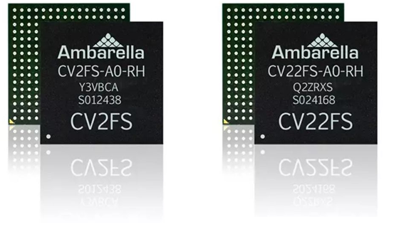
The CV22FS and CV2FS CVflow architecture provides computer vision processing capabilities at 8-megapixel or higher resolution at a frame rate of 80 frames per second, enabling long-distance and high-precision target recognition. Each system chip includes a dense optical flow accelerator for simultaneous localization and mapping (SLAM) as well as estimating distance and depth. Multi-channel high-speed sensor inputs and Ambarella’s image signal processing (ISP) channels provide the necessary support for camera inputs. Ambarella plans to provide samples of CV22FS and CV2FS to customers in the first half of 2020.
15. Intel/Altera FPGA-based SoC
Intel acquired Altera in 2015. Currently, Altera’s autonomous driving FPGA chips are in mass production. Altera’s FPGA products are divided into four major series, including the high-end Stratix series (nearly $10,000), the cost-performance balanced Arria series ($2,000-$5,000), the budget-friendly Cyclone series ($10-$20), and the MAX series CPLD.
Waymo adopts a solution combining Intel CPUs and Altera FPGAs to address the data fusion and algorithm processing required for autonomous driving. The zFAS domain controller equipped in Audi’s new A8 model uses the FPGA chip provided by Altera—Cyclonev SoC.
16. Google TPU
TPU, Tensor Processing Unit, is a custom ASIC chip designed by Google specifically for machine learning. It is optimized for accelerating and scaling machine learning workloads using TensorFlow programming. Google officially released TPU1 at the developer I/O conference in May 2016 and launched TPU2, also known as Cloud TPU, in 2017. TPU2 can be used for both training and inference. Each Cloud TPU consists of four custom ASICs, with a single Cloud TPU achieving a floating-point computing capacity of 180 teraflops (trillions of operations per second) and a memory bandwidth of 64GB.
In 2018, TPU 3.0 was released, offering an 8-fold performance improvement over TPU 2.0. In July 2018, Google also released the Edge TPU chip to capture the edge computing market.
At the Google I/O developer conference in May 2019, Google replaced the fourth-generation TPU, which was supposed to appear at the conference, with a TPUv3 Pod consisting of 1,000 TPUv3s; new plans regarding TPU are not yet known.
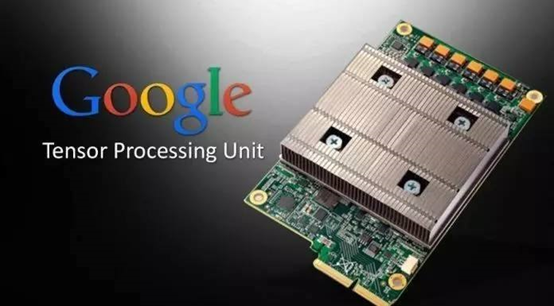
TPUs have been specifically trained for deep machine learning, accelerating the operation of Google’s second-generation AI system TensorFlow, and their efficiency far exceeds that of GPUs. Google’s deep neural networks are driven by the TensorFlow engine. TPUs require fewer transistors for each operation, leading to higher efficiency.
Compared to CPUs and GPUs of the same period, TPUs can offer performance improvements of 15-30 times and efficiency improvements (performance/watt) of 30-80 times.
17. NXP S32V Series SoC
NXP has developed an autonomous driving development platform, BlueBox, based on its second-generation vision-specific processing chip S32V234, integrating the S32V234 automotive vision and sensor fusion processor, LS2084A embedded computing processor, and S32R27 radar microcontroller.
The S32V234 vision processor features a CPU (4 ARM Cortex A53 and 1 M4), 3D GPU (Vivante GC3000), and vision acceleration units (2 APEX-2 vision accelerators), supporting four camera inputs. It can be used for front and rear view cameras, surround systems, and sensor fusion systems, achieving real-time 3D modeling with a computing power of 50 GFLOPs. Additionally, the S32V234 chip has reserved interfaces to support millimeter-wave radar, lidar, and ultrasonic sensors, enabling multi-sensor data fusion, and can support ISO26262 ASIL-C standards.
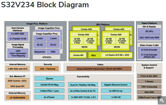
The LS2088A embedded processor is responsible for high-performance calculations, comprising eight 64-bit ARM Cortex-A72 cores, paired with a customized accelerator operating at 2GHz, high-performance communication interfaces, and DDR4 memory controllers, ensuring extremely low latency.
Due to design architecture issues, the NXP S32234 chip suffers from insufficient computing power and lacks a robust ecosystem toolchain, leading to its marginalization. Recently, it has been reported that NXP is collaborating with TSMC to leverage TSMC’s enhanced 5nm technology to develop a new generation of automotive-grade chips expected to launch in 2021. This move presents an excellent opportunity for NXP to regain a leading position in the automotive chip industry.
18. TI TDAx Series SoC
TI’s autonomous driving chip solution is based on DSP, primarily targeting the ADAS market. Its main products are the TDAx series, including TDA2x, TDA3x, TDA2Eco, and the recently released TDA4VM, based on a heterogeneous hardware and generic software architecture. The TDA2x was released in October 2013, primarily aimed at the mid to high-end market, configured with two ARM Cortex-A15 cores and four Cortex-M4 cores, two TI fixed-point C66x DSP cores, and four EVE vision accelerator cores, mainly used for front camera information processing, including lane departure warnings, collision detection, adaptive cruise control, and automatic parking systems.
The TDA3x was released in October 2014, primarily targeting the mid to low-end market, reducing the dual-core A15 and SGX544 GPU, mainly applied in rear cameras, 2D or 2.5D surround views, etc.
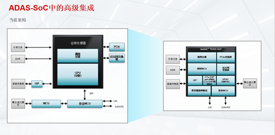
At CES 2020, TI launched the TDA4VM processor series based on the Jacinto™7 architecture, integrating TI’s industry-leading DSP and EVE cores into a single high-performance core, adding floating-point vector computing capabilities. This SoC can execute high-performance ADAS computations with power efficiency using only 5 to 20W of power, eliminating the need for active cooling.
19. Renesas R-Car V3H
R-Car is a series of system-on-chips (SoCs) designed by Renesas Electronics Corporation specifically for autonomous driving vehicle computing, primarily used in automotive information systems. Renesas launched the new R-Car V3H SoC in 2018. The R-Car V3H provides powerful computing performance and AI processing capabilities for automotive front-view vision systems with low power consumption, suitable for L3 and L4 level autonomous driving. The R-Car V3H is optimized for stereo front-view camera applications, achieving five times the computer vision performance of the R-Car V3M SoC launched in April 2017.
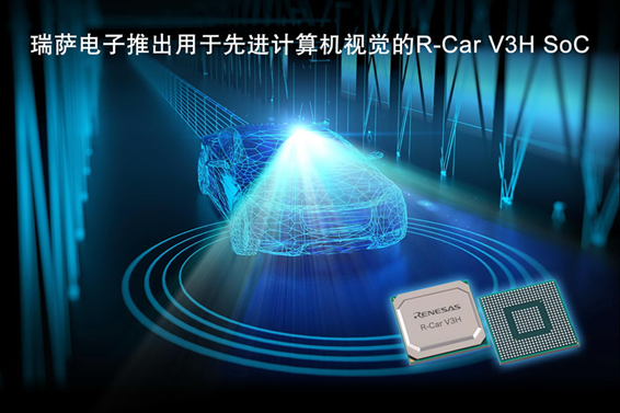
The R-Car V3H SoC focuses on optimizing computer vision processing architecture, supporting all ADAS-related functions from conditional autonomous driving to highly autonomous driving. It employs Renesas’ heterogeneous computer vision core concept based on the IMP-X5+ image recognition engine and dedicated hardware accelerators, implementing advanced perception functions through algorithms including dense optical flow, dense stereo disparity, and object classification. The integrated CNN IP accelerates deep learning with an industry-leading low power consumption of only 0.3W, achieving twice the deep neural network performance of the R-Car V3M.
20. Arm Autonomous Driving Chip Cortex-A76AE
As a mobile chip foundational technology company, Arm does not manufacture chips but researches core technologies for microcontroller chips and licenses them to major chip manufacturers.
Since 1996, general-purpose and real-time processors produced by Arm have been used by major vehicle manufacturers. Now, Arm’s semiconductor intellectual property (IP) is widely applied in ADAS systems (such as collision avoidance, cruise control, etc.), connectivity, infotainment, powertrain control, and other automotive components.
In September 2018, Arm launched its “Safety Ready” program aimed at providing solutions for autonomous vehicles and introduced the Cortex-A76AE product, the first processor designed specifically for autonomous vehicles.
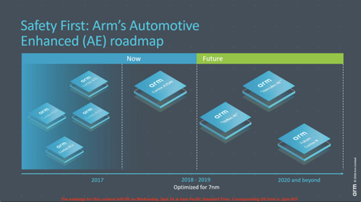
The Cortex-A76AE processor allows chip manufacturers to design chips with safety features, enabling autonomous vehicles to meet the strictest safety requirements, applying features such as automatic evasion. AE stands for “Automotive Enhanced”. This processor, manufactured using TSMC’s 7nm process technology, features a 16-core Cortex-A76AE SoC with computing performance exceeding 250 KDMIPS and a power consumption of 30W, sufficient to meet current application demands. If users require higher performance, they can build more cores or even multiple SoCs. This core incorporates all functional features of the Arm v8.2 microarchitecture, including reliability, availability, and maintainability, and uses a split-lock mode to ensure reliability.
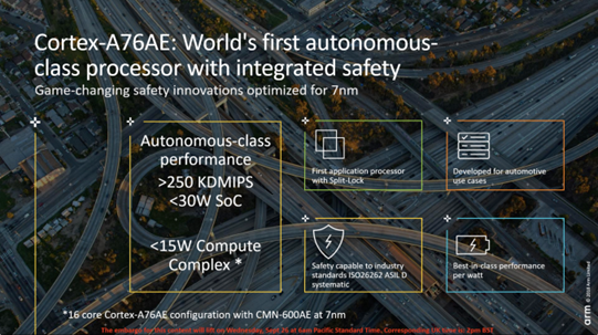
Moreover, SoCs based on the Cortex-A76AE can scale up to 64 cores. In addition to general-purpose computing cores, Arm’s autonomous computing complexes also integrate Mali-G76 GPUs, ARM’s ML processors, and other necessary IPs. Additionally, all complexes support Arm’s memory virtualization and protection technologies, allowing for seamless operation of ML and NN accelerators.
After the Cortex-A76AE, Arm also launched a new processor product adapted for autonomous driving, the Cortex-A65AE. According to Arm’s plan, the first vehicles using the Cortex-A76AE processor will be on the road in 2020, and the Cortex-A65AE will also be launched in 2020.
21. Qualcomm Snapdragon Ride
Qualcomm previously disclosed its plans to develop autonomous vehicle chips in 2017, but due to regulatory reasons, its acquisition of Dutch NXP was unsuccessful in 2018. On January 5, 2020, Qualcomm unveiled the new autonomous driving platform Snapdragon Ride at the Consumer Electronics Show (CES) in Las Vegas, aiming to handle various tasks required for autonomous driving, such as lane control and automatic parking, with expectations for deployment in 2023.
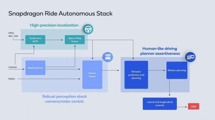
According to Qualcomm, the Snapdragon Ride platform is built on a series of different Snapdragon SoCs and accelerators, adopting a scalable and modular high-performance heterogeneous multi-core CPU, energy-efficient AI and computer vision engines, and industry-leading GPUs. Based on different combinations of SoCs and accelerators, the platform can match the needs of each segment of the autonomous driving market, providing industry-leading thermal efficiency, ranging from devices with 30 TOPS for L1/L2 level applications to devices with over 700 TOPS for L4/L5 level driving, with a power consumption of 130W. Thus, the platform can support passive or air-cooled thermal designs, reducing costs, enhancing reliability, eliminating the need for expensive liquid cooling systems, simplifying vehicle design, and extending the range of electric vehicles. The Snapdragon Ride series of SoCs and accelerators are designed for functional safety ASIL-D level (Automotive Safety Integrity Level D) systems.
Snapdragon Ride is expected to be delivered to automotive manufacturers and Tier 1 suppliers for preliminary development in the first half of 2020. Qualcomm Technologies anticipates that vehicles equipped with Snapdragon Ride will enter production in 2023.
3. Conclusion on Domestic AI Chips
In recent years, Chinese companies have experienced an explosive trend in exploring AI chips, with leading enterprises such as Huawei, Horizon, Cambricon, Westwell, and Baidu, along with other domestic companies focusing on artificial intelligence, voice recognition, and visual processing, such as SemiDrive, Black Sesame, Zhongxing Microelectronics, Bitmain, and Hangzhou Zhongtian Microelectronics. Overall, Chinese companies have already secured several positions in the AI chip field, and the performance and power consumption of Chinese autonomous driving chips are not inferior to foreign chips. However, to reach world-leading levels and even surpass NVIDIA, Tesla, TI, and Xilinx, there is still a long way to go. From R&D design to actual mass production, in-depth testing and validation, and accumulation are also required.
First, domestic chip companies must be prepared for long-term R&D investment, which means spending money and time. There are countless challenges to overcome in AI chip R&D without prior accumulation. This long-term investment reflects both significant financial input and a positive cycle of high output; on the other hand, it requires continuous accumulation and high tolerance in chip architecture design, underlying software, and operating system design capabilities.
Second, as the Chinese saying goes, “too many cooks spoil the broth.” If domestic chip companies want to share the cake in the AI chip field or even surpass international competitors, they must focus on one vertical field, truly delve into it, and provide a comprehensive solution and product to users, offering a product ready for mass production rather than just a DEMO; it must be genuinely applicable.
Third, establishing an ecosystem is crucial. Foreign chip companies generally have their own systems and ecosystems. Huawei can quickly launch series of chips like Kirin, Ascend, and Kunpeng based on its years of ICT accumulation, but it still lacks in ecological aspects, reflecting in software, operating systems, architecture, auxiliary components, toolchains, etc. Therefore, domestic chip manufacturers must establish an ecosystem related to AI chips and cultivate a user system. For example, NXP and Intel have developed curriculum and certification systems in domestic universities for many years, and Huawei has also consciously carried out strategic cooperation with universities and research institutions in recent years; this initiative will undoubtedly have far-reaching effects.
Fourth, regarding process technology, we know that last year’s incident with ZTE facing chip supply interruptions and Huawei encountering issues with chip suppliers due to US sanctions are significant challenges. This primarily involves the chip process technology; the mainstream level of chip manufacturing processes is 7-14nm, while TSMC has long since mass-produced 7nm chips, and the 5nm process has also entered mass production, currently researching 2nm technology. Chinese chip companies can only achieve 14nm, and only SMIC can handle this, leading to a lack of ability to produce the most advanced 7nm and smaller chips. Currently, the issues Huawei faces are also challenges the entire Chinese chip industry faces. Although the possibility of Huawei circumventing US sanctions is low, the key question is how quickly Chinese chip companies can establish world-class process manufacturing capabilities domestically.
While we are optimistic about the development of the Chinese chip industry, achieving world-class levels in AI chips or even surpassing them is still a long way off. The artificial intelligence industry has catalyzed this process, but talent cannot replace experience; accumulation is equally important, especially since domestic enterprises have been lacking in this regard. Whether they can quickly catch up and surpass depends on how domestic enterprises exert their efforts.
Album: Video: Latest Computer Vision Applications/Papers/Open Source
Album: Introduction to Computer Vision
Album: Introduction to Visual SLAM
Album: Latest SLAM/3D Vision Papers/Open Source
Album: 3D Vision/SLAM Open Course
Album: Principles and Applications of Depth Cameras
Album: Analysis and Applications of Dual-Camera Technology in Mobile Phones
Album: Camera Calibration
Album: Panoramic Cameras
Learn SLAM from 0 to 1, click ↓
Visual SLAM text + video + Q&A + learning path planning!

Exchange Group
Welcome to join the WeChat reader group to communicate with peers; currently, there are SLAM、3D Vision、Sensors、Autonomous Driving,Computational Photography、Detection, Segmentation, Recognition, Medical Imaging, GAN、Algorithm Competitions and other WeChat groups (which will gradually be subdivided), please scan the WeChat ID below to join the group, noting: “Nickname + School/Company + Research Direction”, for example: “Zhang San + Shanghai Jiao Tong University + Visual SLAM”. Please follow the format; otherwise, you will not be approved. After adding successfully, you will be invited to relevant WeChat groups based on your research direction. Please do not send ads in the group; otherwise, you will be removed from the group. Thank you for your understanding~

Submissions and collaborations are also welcome: [email protected]

Long press to follow Computer Vision Life