NOR Flash and NAND Flash are two mainstream types of non-volatile memory (data is retained after power loss). Although both are based on floating-gate transistor structures, they exhibit significant differences in design, performance, and application scenarios.
1. Storage Structure and Access Method
-
NOR Flash
-
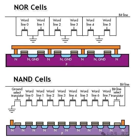
Parallel Structure: Storage cells are independently connected, supporting random access (similar to memory), allowing any byte to be read directly via address lines.
-
Execute In Place (XIP): Code can run directly on NOR without needing to load into RAM, suitable for scenarios requiring high real-time performance (e.g., boot code).
-
NAND Flash
-
Serial Structure: Cells are connected in a chain, requiring sequential access by page (Page, typically 4KB) or block (Block, 128KB–4MB).
-
Controller Dependent: Requires a dedicated controller to manage addressing, with a complex interface (e.g., 8/16-bit multiplexed bus).
2. Performance Comparison
| Metric | NOR Flash | NAND Flash |
|---|---|---|
| Read Speed | Fast (random read 50–100ns) | Slow (page read 25–50μs, a thousand times slower than NOR) |
| Write/Erase Speed | Slow (erase takes 5ms–1s, must first write all 0s) | Fast (erase only 2–4ms, supports bulk operations) |
| Erase Unit | Larger (64–256KB) | Smaller (8–32KB), more flexible |
3. Capacity and Cost
-
NOR Flash
-
Small capacity (typically 1MB–1GB), low density due to independent cell connections.
-
High cost (price per unit capacity is 10–20 times that of NAND).
-
NAND Flash
-
Large capacity (GB–TB level), small cell size and supports 3D stacking (e.g., 238-layer technology).
-
Extremely low cost (QLC as low as $0.03/GB).
4. Reliability and Lifespan
-
Reliability
-
NOR: Very few bad blocks, almost no error correction (ECC) needed, data retention up to 20 years.
-
NAND: Factory bad block rate of 1%–2%, requires ECC and bad block management (BBM), more frequent bit flips.
-
Lifespan:
-
NOR: Approximately 100,000 erase/write cycles (SLC type).
-
NAND: SLC up to 100,000 cycles, but MLC/TLC drops to 300–500 cycles.
5. Interface and Usability
-
NOR Flash
-
SRAM interface, separate address/data lines, directly mounted on CPU bus, can run code without drivers.
-
NAND Flash
-
Complex I/O interface (e.g., ONFI/Toggle), requires MTD driver, FTL layer (logical address mapping), wear leveling algorithms.
-
Easy to upgrade (standardized interface, flexible capacity expansion).
6. Typical Application Scenarios
| Scenario | Recommended Type | Reason |
|---|---|---|
| Embedded Boot Code (BIOS/U-Boot) | NOR Flash ✅ | Supports XIP, fast random reads. |
| Real-Time Operating System (RTOS) Firmware | NOR Flash ✅ | High reliability, low latency. |
| Large Capacity Storage (SSD/USB Drive/Smartphone) | NAND Flash ✅ | High density, low cost, high-speed writing. |
| Industrial Sensor Logging | NAND Flash ✅ | Efficient sequential writing, large capacity requirements. |
7. Conclusion:
-
Choose NOR when: direct code execution is needed, fast boot (e.g., automotive ECU), small capacity (≤1GB), and high reliability is a priority.
-
Choose NAND when: large capacity storage (data/media files) is needed, cost-sensitive, and can tolerate complex controllers (e.g., FTL in SSDs).
Modern systems often combine both: NOR stores boot code, NAND stores main data, balancing performance and cost. Technological advancements are pushing NOR to develop below 40nm processes (capacity increased to 4Gb), while NAND is breaking through the TB-level bottleneck through 3D stacking.