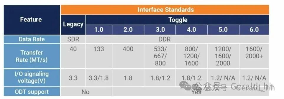
The two most prominent public interface standards for NAND Flash technology are the Open NAND Flash Interface (ONFI) and the Toggle standard. While comparisons can be made between these two standards, a recognized “common point” is the JESD230 standard published by the Joint Electron Device Engineering Council (JEDEC), which defines the interoperability standards for NAND flash device interfaces.
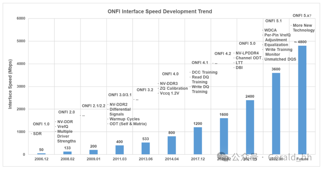
ONFI Interface
In 2006, a large group of technology companies including SK Hynix, Intel, Micron, SanDisk, Phison, and Sony established the Open NAND Flash Interface (ONFI) working group. Later that year, the first version of the ONFI standard was drafted and released, aiming to provide a unified standard to address the chaotic nature of the flash memory market (stemming from inconsistencies in flash interface standards among storage products, flash suppliers, and downstream product manufacturers). Today, the ONFI working group continues to release updates to expand the standard set, which has now evolved to ONFI 5.2.
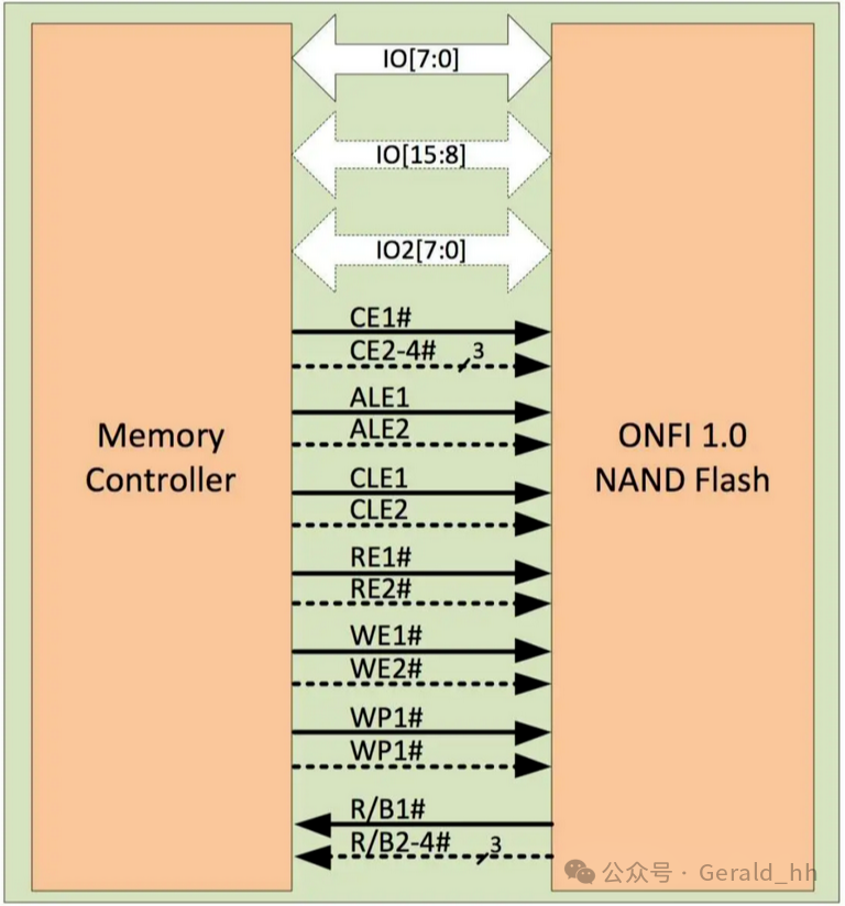
ONFI 1.0
The initial version of the ONFI specification aimed to standardize the pin assignments and commands for NAND flash. The electrical interface of ONFI NAND v1.0 is similar to traditional NAND interfaces but adds some options to support emerging technologies at the time. ONFI v1.0 introduced options to support a 16-bit data bus or an additional independent 8-bit data bus and control signals to support up to 4 dies in one package. To connect with controllers using different logic voltages, an optional voltage rail (VDDQ) was also added as the input power for the input/output interface. The achievable maximum throughput is approximately 50 MBps, which is about a 20% improvement over traditional NAND flash.
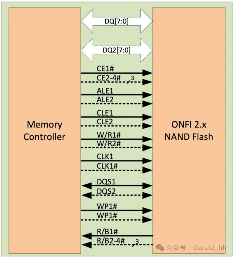
ONFI 2.0/2.1/2.2/2.3
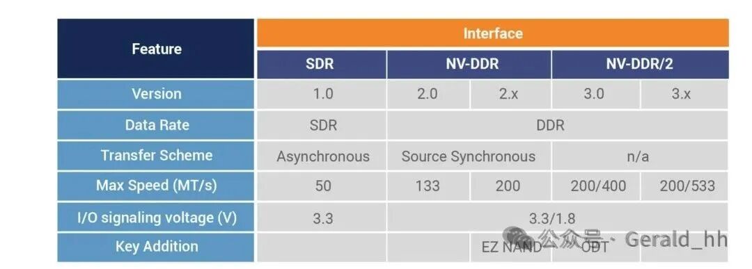
ONFI 2.0 was released in February 2008. The most significant change was the adoption of a double data rate (DDR) transmission scheme, which greatly increased the maximum throughput of devices by allowing data transmission on both edges of the control signal. The interface in ONFI v2.x is referred to as NV-DDR. To ensure backward compatibility, support for asynchronous interfaces was retained, but the changes aimed to support synchronous interfaces. Aside from some minor modifications, most interface signals remain the same as in v1.0. The I/O bus was renamed to DQ bus, a data strobe signal (DQS) was added, WE# became the clock signal (CLK), and RE# became the read/write direction signal (W/R#). Data is transmitted on the rising and falling edges of the DQS signal to achieve double data transfer rates.
In ONFI 2.0, the maximum throughput increased to 133 MBps, and ONFI 2.1 was approved in January 2009, which included numerous new features to provide speeds of 166 MB/s and 200 MB/s, along with other enhancements to improve power, performance, and ECC functionality. The electrical interfaces and throughput of ONFI 2.2 and 2.3 remained unchanged; these updates mainly focused on optimizing commands to improve efficiency in large systems and support for ECC ZERO NAND (EZ-NAND) interfaces.
ONFI NAND v3.x and v4.x Interfaces
ONFI 3.x
ONFI 3.0 was released in March 2011, significantly increasing the supported transmission rate to 400MT/s, and the signal voltage was reduced to 1.8 V, resulting in better power consumption performance. Differential signal support was provided for DQS and RE# signals, and on-die termination (ODT) and VREF voltage support were added.
ONFI 3.2 was released in June 2013, raising the NV-DDR2 I/O speed to 533 MT/s and introducing multi-channel packages (BGA-316 and BGA-272) to support small SSDs.
ONFI 4.0
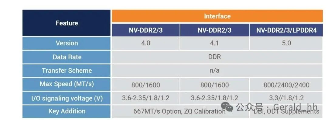
ONFI 4.0 was released in April 2014, introducing the NV-DDR3 interface with a working voltage of VccQ = 1.2V to enhance performance and improve power consumption, extending NV-DDR2 and NV-DDR3 I/O speeds to 667 MT/s and 800 MT/s. A technique called ZQ calibration was also introduced as an ODT aid to calibrate the termination resistance. This involves connecting a high-precision 300-ohm resistor externally for calibration, addressing signal integrity issues caused by internal resistance drift due to voltage or temperature changes.
ONFI 4.x
ONFI 4.1 was released in December 2017, extending NV-DDR3 I/O speeds to 1066MT/s and 1200MT/s. To achieve better signaling performance, ONFI 4.1 added Duty Cycle Correction (DCC), Read and Write Training (for speeds exceeding 800MT/s). An optional setting of 37.5 ohms was added on top of the 35-ohm driver strength from 4.0. To reduce power consumption, support for 2.5V Vcc was added, along with a series of configurations ranging from 2.35V to 3.6V on top of the existing 3.3V/1.8V/1.2V settings.
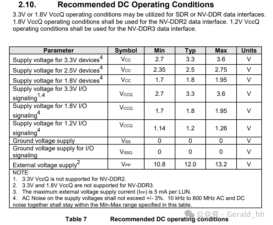 ONFI 4.2 was released in February 2020, extending NV-DDR3 I/O speeds to 1333MT/s, 1466MT/s, and 1600MT/s.
ONFI 5.0
ONFI 5.0 was released in May 2021, extending NV-DDR3 I/O speeds to 2400MT/s. It introduced a new low-power NV-LPDDR4 interface, reducing overall power consumption while increasing the transmission rate per interface, reaching speeds of up to 2400MT/s. With the NV-LPDDR4 interface, an optional data bus inversion (DBI) feature was defined to further manage power consumption. New smaller package sizes BGA-178b, BGA-154b, and BGA-146b were added.
On the other hand, the emergence of NV-LPDDR4 has once again driven improvements in ODT functionality. Additional features such as ODT disable/enable and Channel ODT address the potential impact of the new NV-LPDDR4 interface on ODT.
When NV-LPDDR4 is enabled, the internal reference voltage between the NAND device and the controller can be in an untrained state, but small signal fluctuations caused by ODT may lead to command sequence failures. Therefore, timely disabling/enabling of ODT can significantly affect operations under the new interface.
In addition to this switch-like functionality, Channel ODT settings also grant control over the pull-up resistor strength on NAND outputs, thereby granting control over the signal termination resistance. In other words, this setting essentially allows the host side to determine the optimal ODT strength within each channel during data output operations. Meanwhile, the NAND device will adjust accordingly based on vendor-specific setting values.
ONFI 5.1
ONFI 5.1 was released in August 2022, extending NV-DDR3 and NV-LPDDR4 I/O speeds to 3600MT/s. To support faster data rates, ONFI 5.1 introduced write duty cycle adjustment (WDCA), Per-Pin VrefQ adjustment, equalization, and unmatched DQS options.
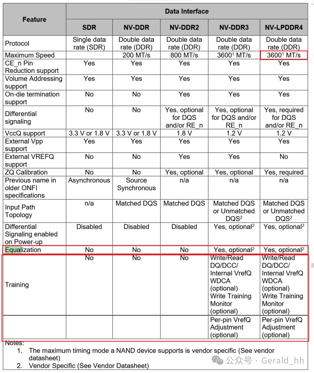
Per-Pin VrefQ adjustment is an optional feature that allows NAND devices to compensate for pin timing variations. NAND vendors can achieve per-pin VrefQ adjustment in one of two ways: by offsetting for per-pin VrefQ adjustment or by absolute settings for per-pin Vref adjustment.
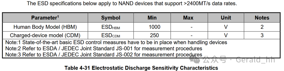
ONFI 5.1 also added ESD specifications.
ONFI 5.2
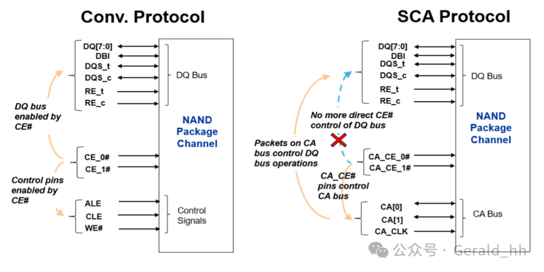
ONFI 5.2 is scheduled for release in October 2024, adding the Single Command Address (SCA) protocol. With the SCA protocol enabled, several signals on the NAND interface will change their functions and/or signal names.
In the Conv. protocol, the CE# signal is renamed to CA_CE# in the SCA protocol to better reflect its SCA functionality. The WE# signal in the Conv. protocol is renamed to CA_CLK in the SCA protocol to better reflect its SCA functionality. The ALE signal, which is only an input in the Conv. protocol, becomes a bidirectional CA[0] signal in the SCA protocol, while the CLE signal, which is only an input in the Conv. protocol, becomes a bidirectional CA[1] signal in the SCA protocol.
When the SCA protocol is enabled, the “CA bus” should collectively refer to the CA[1:0] and CA_CLK signals, while the “DQ bus” should collectively refer to the DQ[7:0], DQS_t, DQS_c, RE_t, and RE_c signals.
Unlike the Conv. protocol, where the DQ, DQS, and RE signals, along with control signals (ALE, CLE, WE#), are enabled/disabled using the CE# signal, in the SCA protocol, the CA_CE# signal only enables/disables the CA bus connected to that CA_CE# LUN, while the DQ bus for those LUNs is enabled/disabled through the data packets on the CA bus.
The Toggle Interface
In the year following the release of ONFI 1.0, the two leading NAND flash manufacturers, Samsung Semiconductor and Toshiba Memory Corporation (TMC), introduced the Toggle interface standard as an alternative to push flash device operations beyond traditional capabilities. Devices using the Toggle interface operate according to a set of scalable, intricately woven guidelines that involve various hardware configurations, signal patterns, and electrical characteristics. The evolution of the Toggle standard occurred within the NAND device specifications released by Samsung and TMC for their customers, rather than being publicly released. This sharply contrasts with the ONFI standard, which is updated and publicly released based on its working group’s consensus.
Toggle 1.0
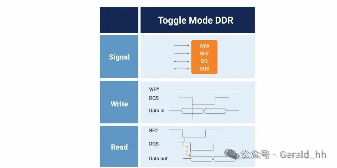
Toggle DDR interface of the first generation shares some common features with ONFI 2.0. Toggle 1.0 uses a bidirectional DQS strobe signal to allow data transfer rates of up to 133MT/s, with each rising and falling edge associated with a single data transfer. However, the distinction between ONFI and Toggle is that Toggle data transfers can occur without a clock signal, making it asynchronous to power consumption that only occurs during read/write operations. ONFI adopted this implementation in version 3.0, which has advantages in power efficiency and design simplicity.
Toggle 2.0 / 3.0 / 4.0
Toggle 2.0 supported devices allow throughput of up to 400 MT/s, comparable to devices running under ONFI 3.0. However, only a portion of Toggle 2.0 devices support ODT functionality based on their release time.
Toggle 3.0 devices were introduced in 2015, supporting transmission rate options of 533MT/s and 667MT/s, and fully supporting ODT and ZQ calibration features, but the mainstream revision of the Toggle standard is the Toggle 4.0 standard. The Toggle 4.0 interface supports transmission rates of up to 800MT/s and 1200MT/s in its earliest versions while matching the necessary features of ONFI.
Toggle 5.0 / 6.0
Toggle 5.0 and 6.0 interfaces are expected to exceed 2400 MT/s in transmission rates, equivalent to over 250 MB/s per die.