As NVIDIA’s GPU creates a $40 trillion market value myth in the cloud computing market, profound changes are also occurring in mobile chip architecture. The NPU, as a dedicated AI engine for mobile SoCs, is becoming a key carrier for deploying models with billions of parameters on the edge, thanks to its architectural energy efficiency advantages.
The NPU is designed specifically for the neural network computations behind large models, achieving breakthroughs in both performance and power consumption compared to CPUs and GPUs. The transition from general-purpose CPUs to dedicated NPUs not only supports new features of AI mobile phones such as real-time semantic understanding and multimodal interaction but also builds an irreplaceable value barrier in scenarios requiring data security and low latency on the edge.
This article will focus on the evolution of mobile processors in two parts: the first part will delve into the demand for edge AI, analyzing the critical role of NPUs in the era of artificial intelligence, and observing how they drive changes in the AI mobile SoC market; the second part will analyze the business model of chip IP design, dissecting ARM’s core positioning logic and its implications for NPU IP vendors.
Table of Contents
1. Technological Changes
2. Industry Trends
1. Technological Changes
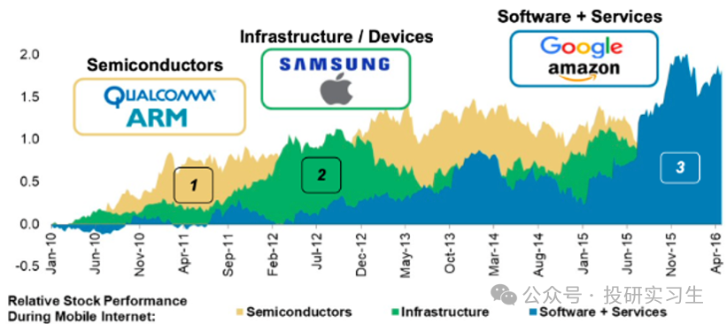
Currently, the functions of AI mobile phones seem to be lacking, one major reason being insufficient hardware performance. Looking back at the mobile internet era, its growth can be divided into three stages: first chips, then devices, and finally software and services. The same logic is now playing out in cloud AI: the large-scale investments in GPUs and data centers over the past two years are transforming into more advanced large models and AI agents.
The core of hardware upgrades for AI mobile phones is the processor, and the key to AI capability within the processor is the NPU. To understand the value of the NPU, we must first discuss the classification and development history of chips.
Chips can be divided into digital chips and analog chips, with digital chips including logic chips and memory chips; the former is responsible for logical operations, while the latter stores data.
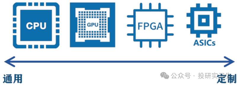
Logic chips can be further divided into four categories: CPU, GPU, ASIC, and FPGA. CPUs and GPUs are more versatile and suitable for handling various tasks, while ASICs and FPGAs are customized for specific needs, offering higher specialization.
The three key elements of AI are algorithms, data, and computing power, with computing power corresponding to hardware. When it comes to AI computing power, the first thing that may come to mind is NVIDIA’s GPU, but that belongs to cloud computing power—CPUs, GPUs, ASICs, and other chips are housed in servers, which then transmit computation results to devices like phones and computers via the network.

Clearly, a whole server cannot fit into a mobile phone, and the data security assurance of cloud computing power is not as strong as that of local computing power on the phone, which is why the highly integrated SoC (System on Chip) has emerged.
The SoC integrates the core components from servers onto a single chip, and due to its advantages of small size, strong performance, low power consumption, and adaptability to complex scenarios, it is widely used in various mobile devices.
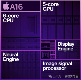
For example, the Apple A16 chip used in the iPhone 14, when opened, typically reveals modules such as CPU, GPU, NPU, memory, and ISP, which are independent chips in PCs and servers, forming a system on the motherboard, while in the SoC, they are integrated into a single chip, hence the name System on Chip.
As mentioned earlier, CPUs and GPUs possess strong versatility and can handle various complex tasks, primarily due to their hardware design characteristics. A CPU consists of an arithmetic unit, a control unit, and cache, processing content that can be divided into instructions (programs) and data, both temporarily stored in memory.
When operating, the CPU follows the von Neumann architecture, sequentially reading instructions and data from memory and executing calculations: instructions enter the control unit, data is sent to the arithmetic unit, and the calculation process is temporarily stored in the CPU’s internal cache, with the results ultimately written back to memory, forming a cycle of fetch → decode → execute → store.
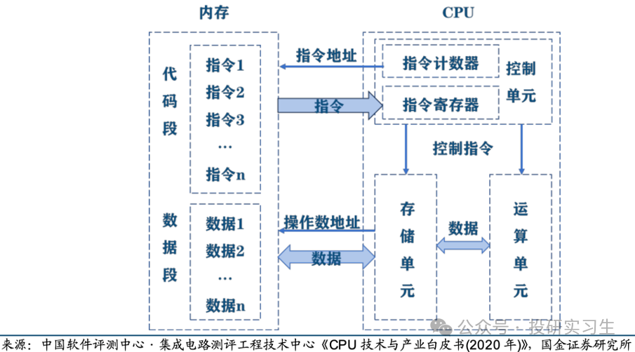
The complete cycle from reading instructions, executing calculations, to writing results is called the instruction cycle, and the number of instruction cycles completed by the CPU in one second is its frequency, a core metric for measuring CPU performance, measured in hertz (Hz)—1 hertz means completing 1 instruction cycle per second.
Increasing CPU frequency can be achieved by adding threads, cores, optimizing architecture, and instruction sets. Adding threads means allowing a core to handle multiple threads simultaneously for different tasks; when one task needs to wait for data (like loading a file), the CPU switches to another thread to handle other tasks, giving the impression of multitasking.
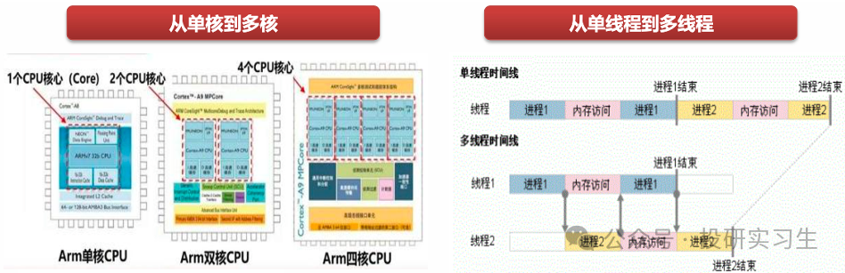
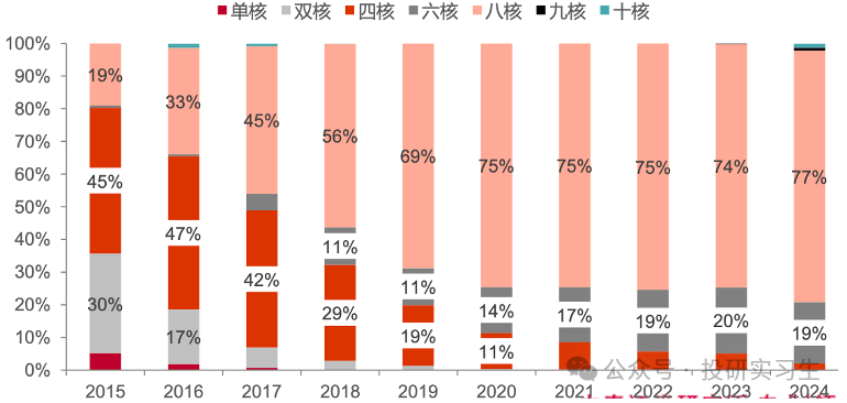
Threads can be seen as an optimization of CPU resource scheduling at the software level, while increasing the number of cores is a physical increase in the number of arithmetic units. With more cores, different tasks can be processed simultaneously, greatly improving efficiency; thus, increasing cores has been one of the main methods for enhancing CPU performance in recent years.
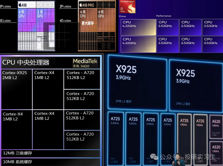
Comparing four flagship SoCs using 3NM technology, the Apple A18 CPU features a 6-core design, while Qualcomm’s Snapdragon 8 Gen 2 and MediaTek’s Dimensity 9400 both have 8 cores, and Xiaomi’s Xuanjie O1 has 10 cores.
Performance is not simply about stacking cores; architecture is also crucial. The core frequencies and caches of the aforementioned companies differ: for example, the Snapdragon 8 Gen 2 has 2 super-large cores at 4.32GHz + 6 large cores at 3.52GHz; although the Xuanjie O1 has 10 cores, it only has 2 super-large cores at 3.9GHz, 4 large cores at 3.4GHz, and the rest are 2 energy-efficient small cores at 1.9GHz and 2 at 1.8GHz, yet their performance is comparable.
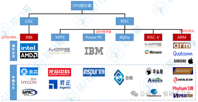
The way hardware resources are called also affects performance, which is determined by the instruction set architecture—it specifies instruction formats, behavior rules, and parameters. Current mainstream architectures are divided into two categories: CISC (Complex Instruction Set Computing) and RISC (Reduced Instruction Set Computing).

CISC is represented by the X86 architecture dominated by Intel and AMD, featuring rich instructions and diverse functionalities per instruction, but with a complex system and lower efficiency, mainly used in desktop and server devices.
RISC, on the other hand, is characterized by simplified instructions, where complex tasks are completed through combinations of multiple instructions, resulting in higher efficiency and lower power consumption, making it standard for mobile devices. The SoCs from Apple, Qualcomm, MediaTek, and Xiaomi mentioned above all adopt the ARM architecture within RISC.
Other mainstream RISC architectures include the open-source RISC-V, but due to its ecosystem being less developed than ARM (which holds a 95% market share), its adoption rate is relatively low; however, it also has promising prospects under the deepening of open-source and the demand for technological autonomy.
The processing characteristics of CPUs endow them with strong versatility, enabling them to handle various complex logical tasks, thus becoming the core computational hub. However, they adopt a serial structure, processing instructions and data sequentially, which limits their efficiency in image and game modeling data processing.
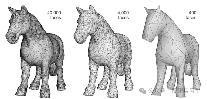
Images consist of massive pixels; for example, a 1080P image contains 1920×1080=2.07 million pixels, and processing a single pixel is not complex; 3D game models consist of multiple geometric shapes, with vertex coordinates stored in memory, and vertex connections can be calculated in real-time using slope and intercept formulas.
Due to the CPU’s serial mode requiring calculations for each pixel point and model vertex one by one, it becomes inefficient when faced with such high-parallel, low-complexity tasks.
To enhance multimedia and gaming data processing capabilities, NVIDIA first launched the GPU in 1999, specifically designed for pixel and vertex acceleration. Unlike the CPU’s serial computation + complex control logic, the GPU adopts a parallel architecture, processing pixels simultaneously through numerous computing units, with simpler control logic.
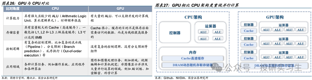
Early GPUs were non-programmable ASIC dedicated processors, only following CPU scheduling to complete image processing acceleration, thereby reducing CPU load.
In 2006, NVIDIA launched the CUDA platform, enabling general programming for GPUs, officially starting the era of GPGPU (General-Purpose GPU), expanding their capabilities to scientific computing, AI, and other fields suitable for parallel computing.
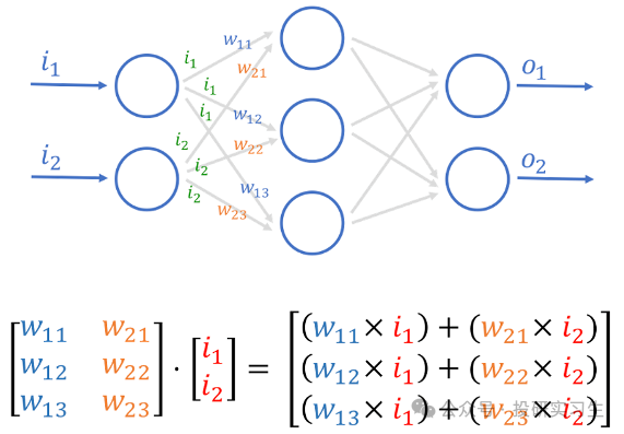
The underlying computational logic of neural networks behind large AI models is simple matrix multiplication, also known as MAC operations (Multiply-Accumulate Operation, a ← a + (b × c)), where the values in the matrix are the model parameters.
Traditional models can suffer from overfitting when the number of parameters is too large, while the existence of Scaling Law under the Transformer architecture means that the larger the parameters, the better the model performs.
Thus, ultra-large (ultra-large parameter) models have been designed, and rapidly and effectively training and using these models requires the parallel computing capabilities of GPUs.
To this end, NVIDIA added Tensor cores to its traditional CUDA cores and RT ray tracing cores in 2017, marking the official transition of its data center business to become the main driver of revenue growth, replacing gaming.
Tensors (multi-dimensional matrices) are the core data structure for AI computing, and Tensor cores achieve this by fusing multiply-accumulate operations (FMA), combining the traditional two-step operation of multiplication followed by addition into one step, allowing matrix operation throughput to reach 12 times that of CUDA cores, becoming a key accelerator for training large models.

However, the versatility of GPUs leads to resource waste when only processing neural network tasks. This is where dedicated ASIC chips designed specifically for AI models come into play, known as NPUs (Neural Processing Units).
The underlying operations of neural networks are MAC operations, but as model parameters increase, the dimensions of tensors can expand dramatically, leading to exponential growth in computation— for example, multiplying an M×N matrix with an N×J matrix requires executing M×N×J multiplications and M×J×(N-1) additions.
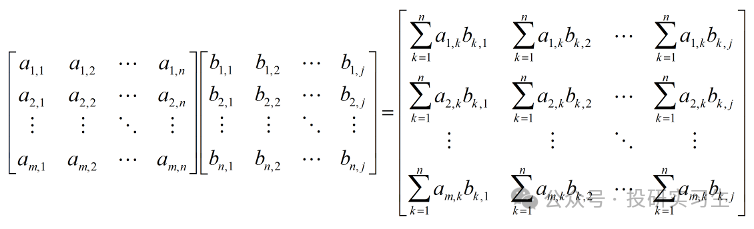
While GPUs can process these computations in parallel through numerous cores, they are not specifically designed for MAC tasks. Their computation flow first parallelizes all multiplications, writes the results to cache, and then reads them back for addition, wasting a lot of time in the process.
Moreover, as memory bandwidth development lags far behind processor performance improvements, computing units frequently wait for data transfers, creating a “memory wall” that severely limits efficiency.
The rigid demands of edge AI inference include privacy and security (data does not leave the edge), low latency (such as real-time image generation), and high energy efficiency (large models running locally require <5W power), which drives the NPU to become a key component of AI mobile SoCs.
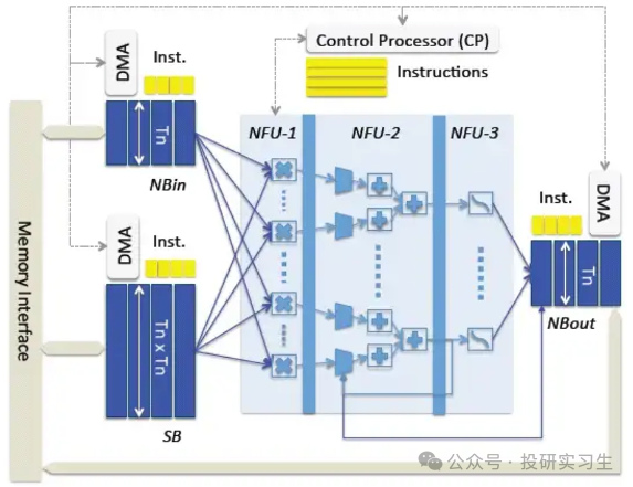
The NPU changes the GPU computing model through hardware architecture innovation, adopting an addition tree design that directly defines multiplication results as addition inputs at the hardware level, eliminating the need to repeatedly write intermediate values to cache and read them back. Compared to traditional MAC architectures, this design, which reduces data movement, can significantly improve energy efficiency.
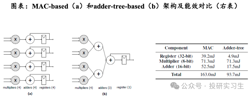
This method of artificially defining data flow rules is designed specifically for MAC operations, but it sacrifices versatility; for example, when calling NPU to compute A*B+C*D*E, the efficiency is not as high as that of a GPU.
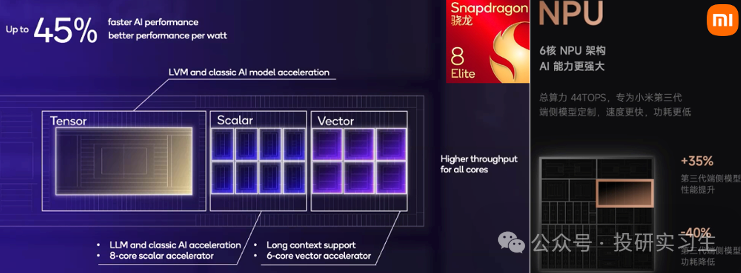
The architectural design of NPUs also differs from GPUs; the basic computational unit of the NPU is the MAC unit designed for the fixed computation flow described above, used for Tensor instructions and operations, but typically also includes Scalar and Vector modules for executing scalar and vector instructions.
For example, in Qualcomm’s NPU, the scalar module acts as an independent computing unit, handling branching, loop control, and conditional logic operations; the vector module is responsible for vector addition, dot products, activation functions, and other operations; while the tensor module consists of MAC units focused on executing matrix multiplications and high-dimensional convolutions.
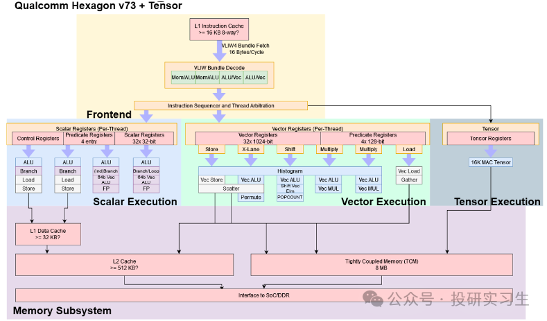
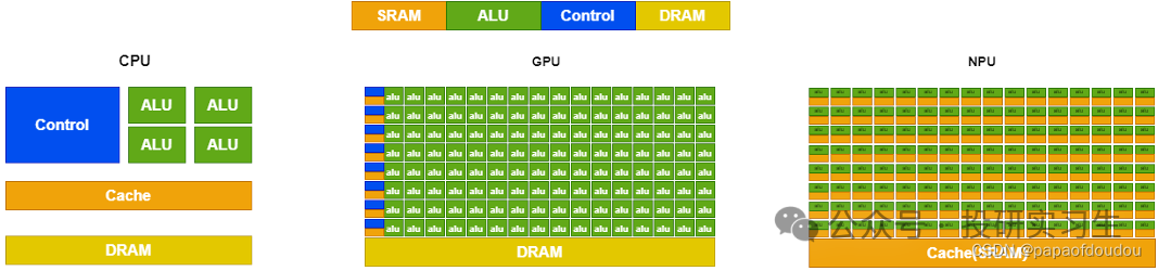
In addition to MAC units, another major innovation in NPUs is tightly coupled memory (TCM), a low-latency on-chip storage technology that reduces the physical distance between MAC and SRAM compared to the distance between ALU and SRAM in GPUs, achieving faster data transfer speeds and lower power consumption.
The computational power requirements for inference and training of large AI models differ significantly, one core aspect being data representation precision. Computers represent numbers in binary 0s and 1s, with more bits leading to higher precision and smaller errors (e.g., the difference between two and four decimal places).
Training trillion-parameter large models requires repeated forward and backward propagation, being sensitive to errors, thus using high precision FP16/FP32, which consumes more energy. However, inference has lower precision requirements, and to balance latency and energy consumption, low precision INT6/INT8 is typically used to enhance energy efficiency while maintaining effectiveness.
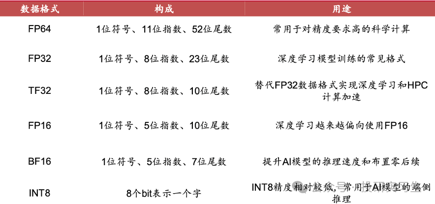
Mobile AI computing focuses on inference, low latency (e.g., facial unlocking, NPU latency <10ms, GPU >30ms), and low power consumption, differing from server/PC scenarios. The NPU is optimized for edge inference needs from an energy efficiency perspective, typically using INT4/INT8 mixed low precision, while introducing dynamic precision adaptation to support different precision levels between neural network layers (e.g., attention layers FP16, MLP layers INT8).
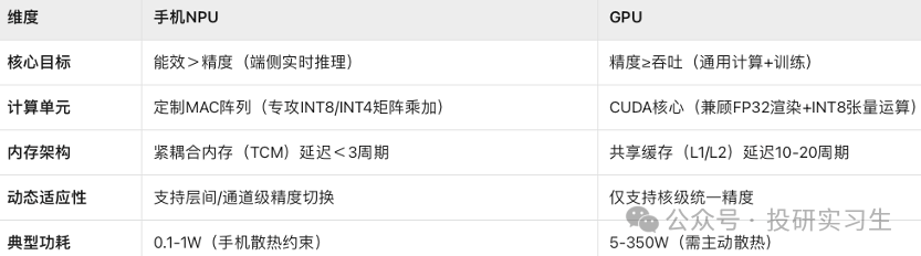
The fixed computation flow, tightly coupled memory, and mixed low precision design of NPUs precisely match the inference needs of mobile AI, making them more suitable for handling mobile AI tasks, achieving real-time responses and low power consumption.
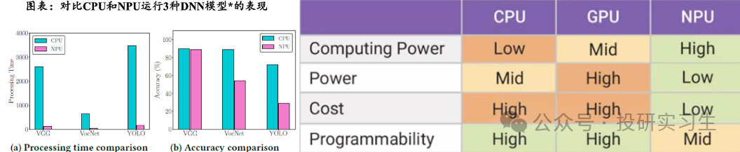
In practice, the computation speed of NPUs far exceeds that of CPUs, with precision comparable to CPUs. In summary, in AI computing, NPUs outperform CPUs and GPUs in performance while consuming less power and cost.
The core metric for measuring NPU performance is TOPS, which refers to the total number of additions and multiplications executed per second. Its calculation formula is: TOPS=2×number of MAC units×frequency/1 trillion. Each MAC unit can perform one addition and one multiplication per clock cycle (hence the multiplication by 2), and frequency determines the number of computation cycles per second, directly affecting the number of operations per unit time.
Thus, increasing the number of MAC units and raising frequency are key ways to enhance NPU performance. For example, Qualcomm’s Snapdragon 8 Gen 2 uses a design of 6-core vector (MAC cores) + 8-core scalar; while the NPU module of Xiaomi’s Xuanjie O1 has only 6 MAC cores, with control and scheduling relying on the CPU.
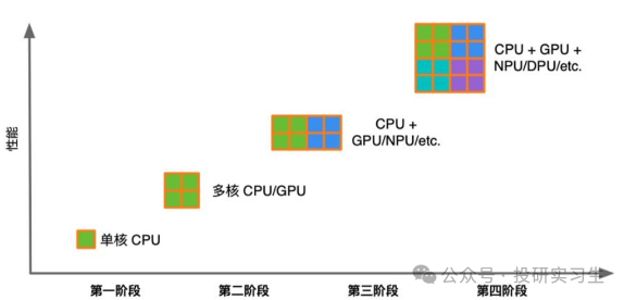
The integration of CPUs, GPUs, NPUs, and other components within the same SoC represents a significant breakthrough in mobile processors, fundamentally differing from traditional discrete designs. In a heterogeneous computing architecture, different types of processors each perform their respective roles, achieving a balance of performance, energy efficiency, and battery life.
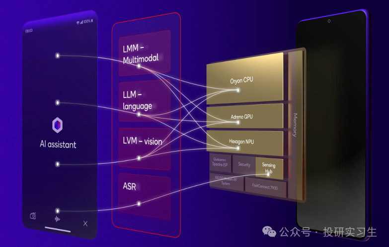
According to Qualcomm’s demonstration, in typical AI mobile usage scenarios, the CPU, GPU, and NPU each have their roles: the CPU is responsible for scheduling control and general computation, the GPU handles image rendering, and the NPU accelerates neural networks.
When a user makes a request, the personal assistant in the phone interacts with the user through voice, images, and videos, with inputs processed by multimodal LMM, language LLM, visual LVM, and speech ASR models before outputting.
Among these, the ASR model runs on the sensor, converting speech to text before passing it to the LLM on the NPU, while simultaneously synthesizing a virtual avatar through the LMM and converting text to speech, with the final rendering of the virtual avatar done by the GPU, all completed within the memory of the SoC.
2. Industry Trends
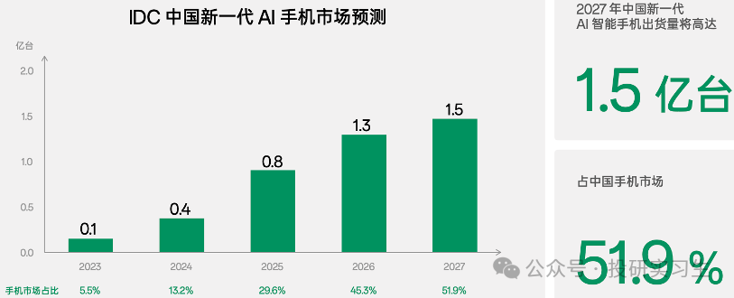
AI photo editing, AI voice assistants, AI summaries, AI search, and many other functions have emerged on our mobile phones, becoming a key component of daily use, and this trend will continue to lead the development of mobile phones as smart terminal devices for many years. According to IDC’s forecast, by 2027, the shipment of AI mobile phones in China is expected to reach 150 million units, accounting for 51.9% of the mobile phone market.
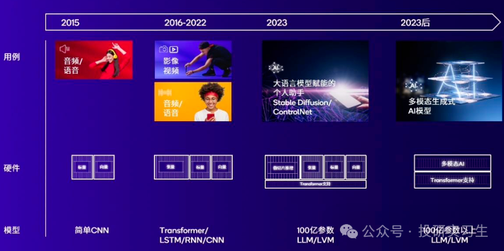
Qualcomm is one of the earliest companies to develop NPUs, launching the first discrete NPU chip, Zeroth, in 2013, and integrating the NPU into the Snapdragon 820 processor in 2015, marking the beginning of the AI heterogeneous computing era.

Early NPUs were primarily designed for AI applications in mobile audio, focusing on scalar and vector operations. Starting in 2016, an increasing number of demands shifted towards photography and video, with the underlying technologies based on complex neural network models such as CNN, LSTM, and Transformer, leading to an expansion of tensor dimensions as parameter counts increased, necessitating more efficient tensor cores to be incorporated into NPUs, optimized specifically for MAC operations.
The design of NPUs focuses on high-speed processing of MAC operations, rapid data transfer from memory, and reducing power consumption, with the addition tree for MAC operations being a key innovation, and its core lies in how to transport data between multiplication and addition. Therefore, how to design the addition tree becomes a key strength for NPU manufacturers.
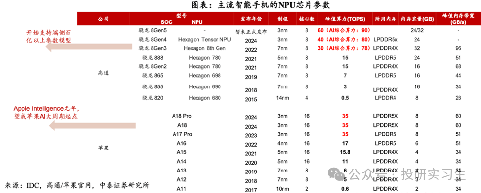
As more large models are deployed on mobile devices, the status of NPUs is continuously strengthening. An AI mobile phone is defined as having an NPU computing power of 30 TOPS, which is the basic threshold for running large AI models.
Currently, most leading SoC manufacturers have reached this threshold, with Qualcomm leading the NPU iteration, having increased the NPU computing power to 40 TOPS in the Snapdragon 8 Gen 2, and is expected to reach 60 TOPS in the upcoming Snapdragon 8 Gen 5.
The semiconductor industry chain consists of three main stages: IC design, chip manufacturing, and packaging/testing, with the design stage holding the highest value, followed by manufacturing, and finally packaging/testing. After decades of globalization, the industry has formed a highly specialized division of labor system, with the two most representative models being IDM (Integrated Device Manufacturing) and Fabless (Fabless Design).
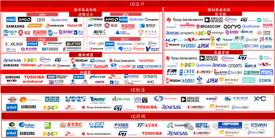
The core feature of the IDM model is that chip companies control both the design and production stages, achieving full-process autonomy from circuit design to wafer manufacturing and packaging/testing. The advantage of IDM lies in the deep collaboration between design and manufacturing processes, allowing for more precise optimization of chip performance and yield, with Intel and Samsung being typical representatives of the IDM model.
The Fabless model focuses on the chip design stage, completely outsourcing manufacturing, packaging, and testing to specialized foundries. Companies like Apple, Qualcomm, NVIDIA, and Huawei HiSilicon adopt this model: they focus on architecture design, algorithm optimization, and other core innovations, while entrusting wafer foundry to TSMC, SMIC, etc., and packaging/testing to companies like JCET and Tongfu Microelectronics.
This model is highly flexible, allowing for rapid responses to market demands without bearing the fixed costs of facilities and equipment, becoming the mainstream model for chip innovation, while the advanced processes of foundries (such as TSMC’s 3nm and SMIC’s 7nm) provide crucial support for the technological breakthroughs of Fabless companies.
The leap in NPU performance within mobile SoCs primarily relies on breakthroughs in chip design capabilities. This includes architectural innovations by SoC manufacturers themselves, such as optimizing MAC unit layouts and designing tightly coupled memory architectures to enhance computational efficiency; it also relies on support from the upstream design ecosystem—design IP (such as ARM’s NPU instruction set licensing) provides a technical foundation for basic computational units.
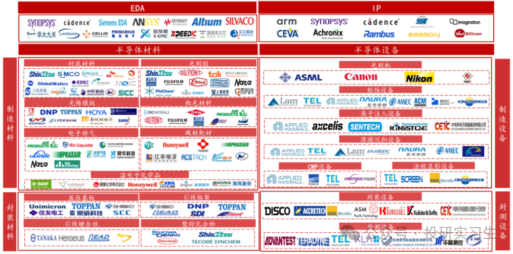
In addition to design, advancements in the manufacturing stage are also key to upgrading NPU performance. Improvements in process technology (such as moving from 5nm to 3nm) allow for more computational units to be integrated within the same area while reducing power consumption per unit, directly enhancing the power density of NPUs.
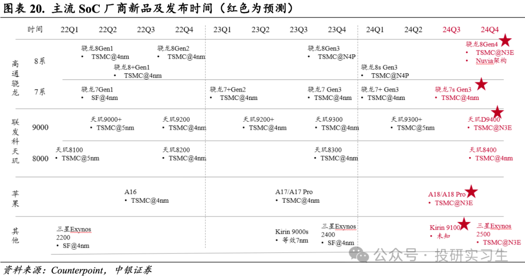
Designing mobile SoCs is highly complex, with only a few companies globally possessing flagship-level design capabilities, including Apple, Qualcomm, Samsung, Huawei HiSilicon, Unisoc, and the emerging Xiaomi Xuanjie, which together dominate the mobile SoC market.
Apple, Samsung, Huawei, and Xiaomi, the four companies capable of designing 3nm mobile SoCs, are also core players in the mobile market, with their chips primarily used in their own phones, while Qualcomm and MediaTek’s chips are used across various Android phone brands.
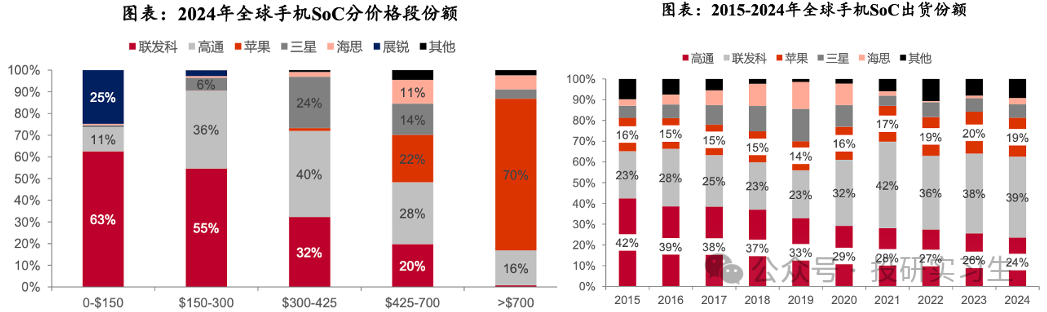
In terms of price segments, MediaTek is the main choice for low-end models, holding over 30% market share in the sub-$425 smartphone market, while Unisoc occupies a quarter of the market for phones under $150. Qualcomm’s chips are mainly used in high-end models, with a strong presence in the $150-$700 price range, while Apple dominates the segment above $700 with the iPhone.
From a market share perspective, Apple consistently holds about 20% of the market due to stable iPhone shipments; Huawei HiSilicon had been expanding its share with the growth of Huawei phone sales before sanctions; MediaTek has steadily increased its share due to its high cost-performance advantage amid economic slowdowns and increased shipments of low-end models; while Qualcomm, focusing on the high-end market, has seen a shrinking share.
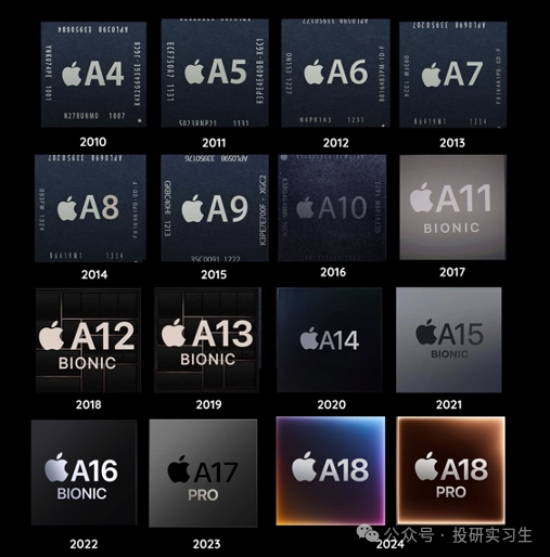
Self-research by mobile manufacturers has become an important development trend in the SoC field, with Apple being a pioneer in this wave. Since launching its first self-developed A4 chip in 2010, Apple has continuously iterated and upgraded its chips, now reaching the A18 series, with its chip performance deeply adapted to the iOS ecosystem becoming a core competitive advantage.
Following closely, Huawei HiSilicon achieved high-end breakthroughs with its Kirin series chips, and now Xiaomi has also officially joined the flagship SoC self-research camp with its Xuanjie series.
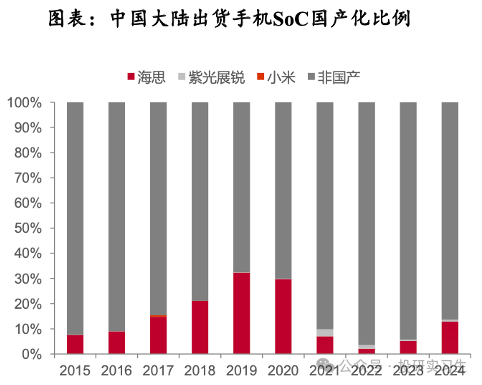
Additionally, localization is another major trend for mobile SoCs. Before 2019, Huawei’s self-developed Kirin chips were the main contributors to localization, but due to sanctions, the localization level of mobile SoCs has continued to decline.
Now, with Huawei’s phone shipments returning to a high-growth trajectory, coupled with technological breakthroughs in self-developed chips like Xiaomi’s Xuanjie O1, and the industry’s heightened awareness of the need for key technology autonomy, the localization level of mobile SoCs is ushering in new opportunities for continuous recovery.
Disclaimer: This article does not constitute investment advice and is for learning and reference purposes only!
References:
· Guojin Securities – Computer Industry Computing Power Deep Report 1: Computing Power Research Framework ~ Full Industry Chain Overview – 2024/04
· Zhongtai Securities – Electronics Industry AI Series on NPU: Neural Network Accelerators Born for Edge AI – 2025/04/20
· Zhongtai Securities – Electronics Industry Xiaomi Conference Interpretation: Ultra-High Performance Self-Developed “Xuanjie O1” Officially Released, A New Starting Point for High-End – 2025/05/22
· Changjiang Securities – Research on AI Edge Chips in Electronic Devices, Instruments, and Components: NPU, Customized Storage Stars in the Sea – 2025/06/13
· Ping An Securities – Semiconductor Industry AI Series Special Report (3): AIoT Edge, Smart Hardware Blooming, Domestic SoC Has Great Potential – 2025/06/19
· Zhongyin Securities – Deep Report on AI Edge: AI Mobile Phones – 2024/06/07
· Qualcomm – Opening Up Terminal-Side Generative AI Through NPU and Heterogeneous Computing – 2024/03/27
· OPPO – AI Mobile Phone White Paper
Welcome to Follow
Investment Research Intern