Introduction to FPGA Internal Resources: Clock Processing Unit

Introduction to FPGA Internal Resources: Clock Processing Unit

The third installment of the basic knowledge of FPGA internal resources is here! Today we will discuss the FPGA clock processing unit module. The clock is the soul of logic, so the clock signal is very important, take note!!Look me~

1. PLL

PLL, the full English name is Phase Locked Loop, which translates to Chinese as lock phase loop. This is because PLL adjusts the frequency and phase of the input clock signal using principles from analog circuits. Therefore, generally speaking, FPGA is not a purely mathematical circuit, as it usually contains a PLL, and it also includes an internal crystal oscillator circuit to generate the clock signal during power-up.The principle structure diagram of PLL is shown in the figure:

Introduction to FPGA Internal Resources: Clock Processing Unit

The principle is as follows: the signal output from the voltage-controlled oscillator VCO is the final output signal of the entire phase-locked loop. This signal is fed back to the phase detector PD (which is also a frequency detector) after being divided by an integer divider. The PD compares the feedback signal with the input reference signal. If there is a difference between them, then PD will output a difference signal. This difference signal is filtered by a low-pass filter F to form a control voltage that changes the frequency of VCO. Under the influence of this control voltage, the frequency or phase of the output signal from VCO will change. If the new output signal, after feedback, equals the reference signal, then PLL enters a locked state; otherwise, PLL remains in an unlocked state, and the above adjustments will continue.

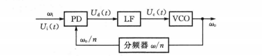
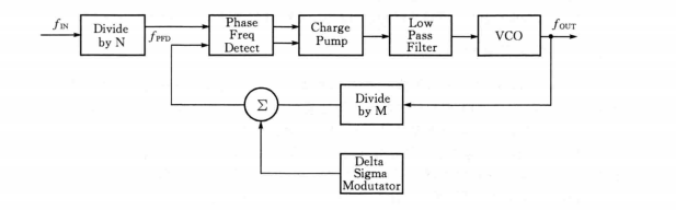
1. Introduction to Xilinx’s Phase-Locked Loop Structure

The basic structure of Xilinx’s phase-locked loop is shown in the figure:

Introduction to FPGA Internal Resources: Clock Processing Unit

We can see that its core circuit completely follows the principle structure diagram of PLL. The output of VCO is not directly supplied to the internal logic, but is output after phase adjustment and division, and such output circuit combinations can have several. Therefore, its output terminals are very flexible, and each output can have different frequencies and phase offsets. Of course, the frequency and phase adjustment steps are determined by the output signal of VCO.

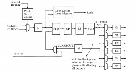
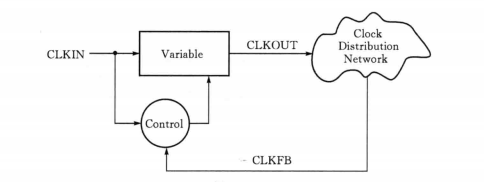
2. Introduction to Altera’s Phase-Locked Loop Structure

The basic structure of Altera’s phase-locked loop is shown in figure 3:

Introduction to FPGA Internal Resources: Clock Processing Unit

We can see that its core circuit also completely follows the principle structure diagram of PLL. In addition, Altera also provides fPLL, which stands for fraction PLL, its principle diagram is shown in the figure:

Introduction to FPGA Internal Resources: Clock Processing Unit

The fraction phase-locked loop is a branch of the phase-locked loop. In traditional phase-locked loops, the output frequency of VCO is generally an integer multiple of the reference clock (note that the reference clock is not the input clock). To obtain a fractional output frequency, we need to add a divider between VCO and the output terminal, just like the Xilinx and Altera PLLs, but the fraction phase-locked loop achieves the ability to directly output a frequency that is a fractional multiple of the reference clock by adding a fine-tuning module Delta Sigma Modulator in the feedback loop between VCO and the phase/frequency detector, thus eliminating the need for a divider circuit at the backend of VCO.

2. DCM

DCM, the full English name is Digital Clock Manager, which translates to Chinese as digital clock manager. Unlike PLL, DCM does not utilize the principles of analog circuits; rather, it adopts a fully digital processing method to handle clock signals. One of the core structures in DCM is DLL, the full English name is delay-locked loop, which translates to Chinese as delay-locked loop. Therefore, its principle is fundamentally different from PLL. Currently, the DLL technology is monopolized by Xilinx, so only Xilinx FPGA chips will have DCM modules. However, with the rapid development of PLL, DLL has gradually lost its advantages due to some inherent defects. Therefore, if Xilinx cannot make breakthroughs in D technology in the short term, then the DCM module may be eliminated in the future. But for now, DCM can still handle the vast majority of design situations. The following is a conceptual diagram of DLL.

Introduction to FPGA Internal Resources: Clock Processing Unit

Here, Variable Delay Line is a variable delay line, which should be composed of several small delay units or buffer gates, and the Control module adjusts the delay time of the variable delay line by comparing the phase relationship between CLKIN and CLKFB, until the phase difference between CLKIN and CLKEB reaches 360 (which means one degree of accuracy), completing the locking.

Chengdian Youth Learning 100-Day Order Class is Hotly Launched!!! Online and offline synchronous learning on the think tank platform.FPGA Introduction Eight Classes”, “FPGA Introduction Ten Projects”, “FPGA Advanced Five Projects”, and other series of courses. The course starts from zero foundation, with each class guiding students through a small experiment, learning the FPGA course step by step.

Introduction to FPGA Internal Resources: Clock Processing Unit

Currently, Chengdian Youth Learning has provided many companies with high-level FPGA talents, with salaries exceeding those of graduates from the same period by 52%, and an employment rate of 100%.

Welfare Giveaway!! You can now apply for free to learn the FPGA course online, hurry up, slow hands will miss out! Course linkhttps://z.shaonianxue.cn. Students can follow the “Chengdian Youth Learning” public account, with the latest updates in the FPGA industry continuing to be updated~~

Introduction to FPGA Internal Resources: Clock Processing Unit
For more information, contact:
Teacher Chen: 13219696129 (WeChat sync)
Teacher Gao: 18935839030
Introduction to FPGA Internal Resources: Clock Processing Unit

END

Introduction to FPGA Internal Resources: Clock Processing Unit

Introduction to FPGA Internal Resources: Clock Processing Unit

Introduction to FPGA Internal Resources: Clock Processing Unit

Introduction to FPGA Internal Resources: Clock Processing Unit

Introduction to FPGA Internal Resources: Clock Processing Unit

Introduction to FPGA Internal Resources: Clock Processing Unit

Leave a Comment