Click the blue text to follow us
Chip
As power semiconductors advance towards the 180-250 nm nodes, with SoC and SiP evolving in parallel, and the fan-in/fan-out wafer-level packaging accelerating differentiation, chip shrinkage has transformed from mere size reduction into a revolution across materials, processes, packaging, and systems: multi-metalization with copper, ruthenium, and molybdenum, extreme packaging pitch of 0.3 mm, 200 W/cm² level three-dimensional heat dissipation, hybrid bonding and FOPLP mass production, along with AI-driven design and testing integration, are collectively reshaping the reliability boundaries, integration density, and cost curves of power devices. This heralds the arrival of a next-generation power packaging era defined by “size reduction + heterogeneous integration + system-level optimization,” which is discussed as follows:
-
Impact of Chip Shrinkage
-
Wafer-Level System on Chip and System-Level Packaging
-
Fan-In and Fan-Out
Impact of Chip Shrinkage
In the continuous evolution of semiconductor technology, the impact of chip shrinkage on the fields of analog and power wafer-level packaging presents multidimensional technical challenges and industrial transformation trends. Compared to traditional wafer-level IC products, power semiconductor devices, which must balance high power density and high reliability requirements, have seen their packaging technology lag behind the iterative pace of digital logic circuits. Current mainstream power devices have migrated from 350nm/500nm technology nodes to 180nm/250nm nodes. Although the significant reduction in chip size has led to increased integration, it has also triggered a fundamental restructuring demand for interconnect systems. As the thickness of copper interconnect layers continues to decrease, the current density per unit area exhibits exponential growth, leading to electromigration (EM) effects becoming a key bottleneck limiting device lifespan. This phenomenon has not only accelerated the development of copper interconnect alternatives but has also prompted the industry to explore the application possibilities of new metallization materials such as ruthenium (Ru) and molybdenum (Mo) to address the reliability degradation issues of traditional aluminum interconnects at sub-micron scales.
At the wafer-level packaging process level, technological iterations are facing dual challenges: on one hand, existing wafer-level solder bump and copper pillar technologies need to overcome the mechanical failure risks caused by excessive growth of intermetallic compounds (IMC) and the reliability issues of voiding at bump interfaces (Kirkendall Voiding) under high-temperature service environments; on the other hand, chip size shrinkage forces the packaging pitch to evolve from 0.5mm to 0.4mm and even 0.3mm, which imposes stricter requirements on photolithography precision, ball placement processes, and the flowability of underfill materials. Notably, by 2025, leading manufacturers such as TSMC have begun piloting hybrid bonding technology, achieving sub-micron pitch interconnections through copper-copper direct bonding, providing a new path for the miniaturization of power device packaging.
Heat dissipation issues, as a derivative challenge of chip shrinkage, are particularly prominent in the power device field. The heat flow density resulting from high power density has exceeded the 100W/cm² level, making traditional silicon-based heat dissipation materials approach their physical limits. The industry is actively laying out three-dimensional integrated heat dissipation architectures, such as embedding microchannel liquid cooling modules directly into packaging substrates or using diamond/silicon carbide composite materials as thermal diffusion layers. Infineon’s recently released third-generation CoolSiC™ MOSFET products successfully control junction temperature fluctuations within ±5°C by integrating phase change materials (PCM) and graphene heat dissipation films, providing a demonstrative solution for high power density applications.
From an industry dynamics perspective, by 2025, the global power semiconductor packaging market is accelerating its shift towards fan-out wafer-level packaging (FOWLP) and panel-level packaging (PLP) technologies to achieve better cost-performance ratios. At the same time, breakthroughs in heterogeneous integration technologies, such as achieving vertical interconnections between power devices and control chips through silicon interposers, are reshaping the competitive landscape of system-level packaging. These technological evolutions not only require the precision of packaging processes to be elevated to the nanometer level but also promote the deep cross-integration of materials science, thermal management engineering, and electromagnetic compatibility design, ultimately shaping the next-generation power packaging paradigm that meets future energy electronics demands.
Wafer-Level System on Chip and System-Level Packaging
In the ongoing evolution of semiconductor technology, the technical paths of System on Chip (SoC) and System in Package (SiP) exhibit distinct complementary characteristics, jointly driving power integrated devices towards higher integration and performance optimization. SoC achieves extreme integration density and energy efficiency by integrating digital, analog, and power devices on a single silicon chip, but its design complexity and process compatibility challenges escalate sharply with process scaling. Taking TSMC’s 2025 technology roadmap as an example, its N2 node enhances logic density by 1.23 times through nanosheet transistors and back-end power supply technology (SuperPowerRail), but faces yield control challenges brought by line widths below 10nm, prompting the industry to turn its attention to heterogeneous integration solutions.
In this context, SiP technology demonstrates unique advantages by vertically stacking chips of different process nodes through 3D packaging technology, effectively balancing performance and cost. Samsung’s GAA process and X-Cube 3D packaging combination, set to launch in 2025, allows the integration of 3nm logic chips with 14nm power devices within the same package, avoiding the high costs of advanced processes while meeting high power density demands. This technological path is particularly significant in the industrial control field, as Intel’s 2025 industrial control white paper shows that PAC controllers using SiP solutions can integrate up to 8 heterogeneous chips, shortening the IT/OT fusion cycle by 40% while reducing system-level power consumption by 25%.
Breakthroughs in thermal management technology provide crucial support for the synergistic development of both. Infineon’s third-generation CoolSiC™ MOSFET, by integrating phase change materials and graphene heat dissipation films, controls junction temperature fluctuations within ±5°C, and this innovation is applied in SiP modules, effectively solving the thermal coupling issues of multi-chip integration. The hybrid bonding technology produced by Qingdao Wuyuan Semiconductor in 2025 achieves 0.4mm pitch interconnections through copper-copper direct bonding, combined with the high thermal conductivity of silicon carbide substrates, enabling power density to exceed 200W/cm².
Market trends indicate that the penetration rate of SiP in the consumer electronics sector is growing at an annual rate of 18%, while SoC still occupies over 90% of the high-end smartphone market. This divergence is particularly evident in the automotive electronics sector: 800V high-voltage platform models generally adopt SiP solutions to integrate SiC power modules, while autonomous driving chips rely on SoC for low-latency computing. As the global power device market size surpasses 100 billion RMB by 2025, this technological complementarity will become increasingly significant, driving the industry towards a dual-track model of “SoC deepening + SiP modularization.”
Fan-In and Fan-Out
In the evolution of semiconductor packaging technology, fan-in and fan-out wafer-level packaging (WLCSP) exhibit significant differentiation in technical paths and market applications, jointly driving the industry towards higher integration and performance optimization.
Fan-in WLCSP, as a representative of traditional wafer-level packaging, occupies an irreplaceable position in the consumer electronics sector due to its technological maturity and process stability. This technology achieves lateral expansion of chip I/O ports through redistribution layers (RDL), supporting extreme miniaturization with a chip size to package size ratio of 1:1, suitable for low I/O count (≤200) and small size (≤6mm×6mm) chips, such as power management ICs in mobile devices. In 2025, the industry focuses on material improvements to enhance thermal cycling performance, such as optimizing RDL line width/spacing from traditional 9/12μm to 5/5μm or even finer widths. Meanwhile, the application of new materials like glass substrates effectively addresses warpage issues, with companies like Shandong Tianyue Advanced making technological breakthroughs in silicon carbide substrates, providing high-performance material support for fan-in packaging. However, its limitations lie in the packaging size being constrained by chip size, making it difficult to meet high I/O density demands, and its cost advantage diminishes in low-yield scenarios.
Fan-out WLCSP, on the other hand, breaks through physical limitations by reconstructing chip layouts, supporting larger package sizes and higher I/O densities. Its core advantage lies in the RDL layer extending outward, allowing for the redistribution of chip surface I/O ports, thus accommodating looser solder ball spacing (such as embedded wafer-level BGA technology). In 2025, panel-level fan-out packaging (FOPLP) becomes the focus of technological breakthroughs, using large-size panels of 600mm×600mm to replace traditional wafers, increasing single wafer capacity by 5 times and reducing costs by over 20%. Companies like TSMC, ASE, and ChipMOS are accelerating the layout of FOPLP production lines, with ASE’s Kaohsiung plant expected to achieve mass production by 2026, and ChipMOS’s 510×515mm panel yield exceeding expectations. The technical challenges of FOPLP focus on process control under large panels, including warpage management, photolithography uniformity optimization, and chip offset suppression. For example, replacing traditional spin-coating processes with lamination/spraying techniques, combined with improvements in the uniformity of metal deposition and plating processes, effectively addresses the processing challenges of large-size panels. Additionally, glass substrates, due to their high flatness and thermal stability, have become key materials supporting the realization of high-density interconnections (such as 2/2μm line width/spacing).
From a market application perspective, fan-in packaging, with its cost advantages and process maturity, still dominates the consumer electronics sector; while fan-out packaging, especially FOPLP technology, is becoming the core carrier for high-density integration and heterogeneous packaging. By 2025, TSMC’s InFO technology has been applied to Apple’s A-series processors, Changdian Technology’s XDFOI™ technology has achieved mass production of 4nm Chiplets, and Qingdao Wuyuan Semiconductor has launched the world’s first 3D-RRAM chip through hybrid bonding technology, marking breakthroughs in fan-out packaging in AI computing power and high-end storage fields. According to Yole data, the compound annual growth rate of the fan-out packaging market from 2022 to 2028 is expected to reach 32.5%, with FOPLP’s share increasing from 2% to 8%, becoming the mainstream solution for high-end applications such as AI GPUs and RF chips.
In the future, the combination of fan-out packaging and 3D stacking technology will further unleash potential. By achieving high-density interconnections between chips through hybrid bonding, fan-out packaging can support multi-chip heterogeneous integration (such as SiP), meeting the stringent bandwidth and low-latency requirements of AI chips. At the same time, the industry is exploring the integration of fan-out packaging with through-silicon via (TSV) technology to construct 3D-RDL intermediary layers, providing more cost-effective solutions for high-performance computing. On the materials side, the large-scale application of new materials such as silicon carbide and glass substrates will continue to drive fan-out packaging towards smaller line widths and higher reliability.
To learn more and enjoy more benefits, you can join our knowledge community, where you can ask questions, and we will do our best to help you!
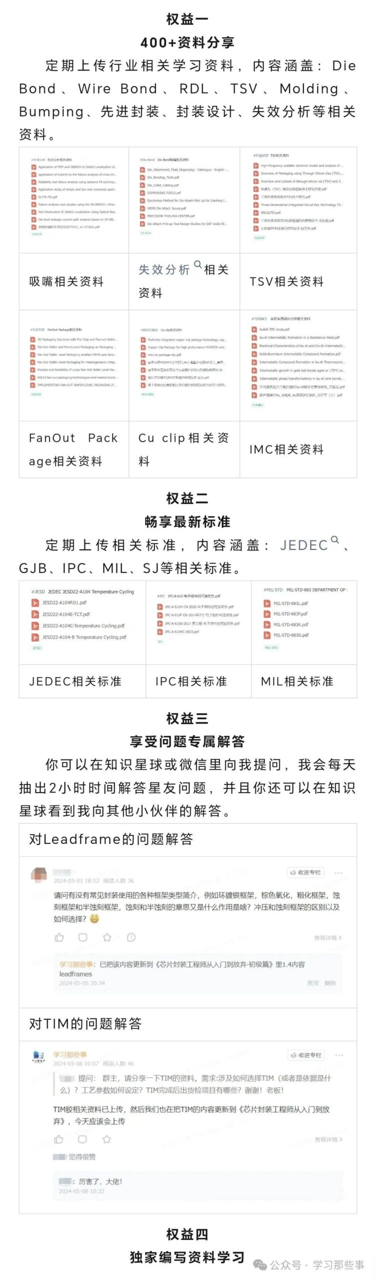
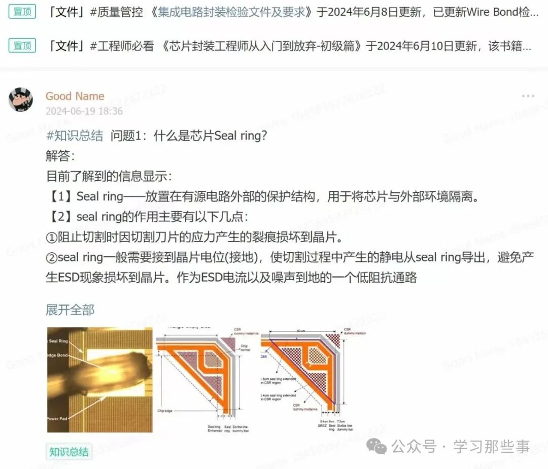

To facilitate communication among peers, this public account has created a series of technical discussion groups, and all colleagues are welcome to join! You can add the group owner on WeChat (WeChat ID: xxnxs999) to apply for group membership!
① Chip Packaging Process Discussion Group
② Failure Analysis and Reliability Discussion Group
③ Quality System Control Discussion Group
④ Advanced Packaging Process Discussion Group
⑤ Wafer Manufacturing Process Discussion Group
⑥ Analog Circuit Design Discussion Group
⑦ Wire Bonding Process Discussion Group
⑧ Packaging Equipment Technology Discussion Group
⑨ Electronic Assembly Technology Discussion Group
⑩ Thinning and Dicing Technology Discussion Group
You can reply to join the group or scan the group owner’s WeChat below to apply for group membership.

That’s all for sharing, if you need anything, feel free to leave a message!

Learning About Those Matters