Follow+Star Public Number, don’t miss the wonderful content
Source | Renesas Embedded Encyclopedia
With the increasing demand for higher functionality and intelligence at the edge and endpoints, these devices also require stronger processing power and larger memory. The functionality of applications is becoming richer, and users demand more advanced features built into their products, including complex graphics and user interfaces, learning algorithms, network connectivity, and advanced security. Currently, machine learning enables voice and visual AI capabilities that help devices make intelligent decisions at the edge and trigger actions without human intervention. Complex software frameworks are an essential component of these solutions.
While processing power is key for all these types of applications, they also drive the demand for fast, reliable, low-power, and non-volatile storage for code and data. When developing embedded systems, the memory choices made by designers can significantly impact performance, cost, design complexity, and power consumption. New architectures are needed to meet the evolving demands for higher performance, larger memory, and lower power consumption while keeping costs low. Close collaboration with memory manufacturers is required to ensure that solutions that meet performance requirements are thoroughly validated. Let’s take a look at various memory architecture options and their best use cases.
Internal Flash or External Memory
Traditionally, general-purpose MCUs used in mid-to-low performance applications have embedded flash memory (typically <2MB) as the preferred non-volatile storage for code. These integrated MCUs are well-suited for most mid-to-low-end IoT applications in various market segments such as industrial or building automation, medical, home appliances, or smart homes. Embedded flash memory has many advantages, including lower latency, lower power consumption, and higher performance, and provides a more integrated solution suitable for simplified, space-constrained applications and low-complexity designs. From a security perspective, it eliminates the attack surface from outside. Therefore, MCUs with integrated embedded flash remain the preferred solution for most applications with lower performance and functionality requirements.
However, embedded flash is costly, and beyond a certain memory density (such as 2MB), costs begin to escalate. Embedded flash is expensive and increases the complexity and cost of MCU wafer processing. The additional manufacturing steps required for embedded flash significantly increase the cost of silicon.
Additionally, MCU manufacturers are increasingly turning to more advanced and finer process geometries, such as 28/22nm or lower, to scale to higher performance and integrate more features on-chip. MCUs with speeds typically ranging from 400MHz to 1GHz are now commonly seen, supporting advanced graphics, analog, connectivity, and security features, as well as advanced security to prevent data/IP theft and tampering. While this addresses performance needs, embedding memory on these devices becomes a challenge because embedded flash does not scale well at lower process geometries, and flash cells cannot be effectively shrunk below 40nm. All of this reduces feasibility or increases costs at lower process geometries.
External Memory
Designers are considering new architectures to bridge this gap and are increasingly using external flash memory for higher-performance applications. Support for more complex use cases (such as high-end graphics, audio processing, or machine learning) drives this demand, while the sharp decline in prices for discrete memory fuels this trend. Using external memory can expand the code and data space in embedded systems since external flash memory is essentially part of the MCU memory mapping and can be read directly for data logging or software storage and execution.
For IoT product manufacturers, using external flash for their high-performance applications offers several advantages, including flexibility in memory size selection and future-proofing their designs. As developers add more features and require larger memory, it is common practice to replace smaller capacity memory with pin-compatible larger capacity memory. It also allows them to adopt a unified platform approach for various designs.
Of course, there are downsides, such as the additional latency involved in accessing external memory (mitigated by using Quad/Octal memory and careful use of caching), slightly higher power consumption, and the additional cost of external memory. It also adds complexity to the circuit board design, requiring additional routing on the PCB and attention to signal integrity.
For MCU manufacturers, separating the MCU from memory enables them to turn to more advanced process nodes for higher performance, more features, and energy efficiency, while reducing their device costs. Most manufacturers now integrate quad or octal SPI interfaces and support execute-in-place (XiP) functionality, allowing seamless connectivity with these NOR flash devices. Some MCUs support dynamic on-the-fly decryption (DOTF), allowing encrypted images to be stored in external flash and securely imported for execution. This solution provides the high performance, low power, and advanced security required for today’s edge applications.
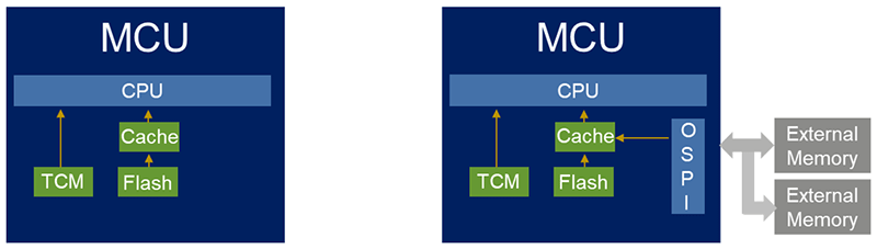
Figure 1. Memory Topology – MCUs with Internal and External Flash
Challenges of External Memory and Link Measures
Of course, external memory also presents challenges, including concerns about the latency associated with external flash and its impact on overall performance. This bandwidth limitation can be mitigated to some extent by using quad or octal SPI interfaces, which allow data to be transmitted over 4 or 8 parallel lines instead of the single-line transmission of conventional SPI. By using double data rate (DDR), throughput can be doubled by sending data on both the rising and falling edges of the clock. External flash manufacturers have also built in support for burst read modes for faster data access, and caching can be used to mitigate some latency impacts, but careful management of software is required to use caching optimally. System designers can also mitigate some latency issues by transferring code to internal SRAM and executing it outside SRAM for maximum performance.
There are also concerns that using external flash will bring higher power consumption, so memory manufacturers pay particular attention to optimizing current consumption for these devices. External memory poses some security risks as it increases the attack surface from outside, creating vulnerabilities that can be exploited by hackers and need to be protected. This requires MCU manufacturers to add encryption/decryption capabilities to Quad/Octal SPI interfaces so that encrypted code can be stored and imported securely.
Using External Flash with RA MCU
Renesas Electronics’ RA series MCUs integrate embedded flash as well as multiple memory interfaces with external memory to provide maximum flexibility and performance. They support quad or octal SPI interfaces, improving data throughput by using 4 or 8 data lines instead of the usual SPI interface lines. This can significantly enhance performance, especially in applications requiring fast memory access (such as graphics, audio, or data logging).
All RA8 series MCUs include an eight-channel SPI interface compliant with the eXpanded Serial Peripheral Interface (xSPI). The xSPI protocol specifies the interface for non-volatile storage devices and achieves high data throughput, low signal count, and limited backward compatibility with traditional SPI devices. Using chip select allows two external memory devices to be connected to the eight-channel SPI interface, providing designers with greater flexibility. Some RA8 MCUs also support dynamic decryption (DOTF), allowing secure import of encrypted images stored in external flash for execution. Figures 2 and 3 show the eight-channel SPI interface on RA8 MCUs, with and without DOTF support.
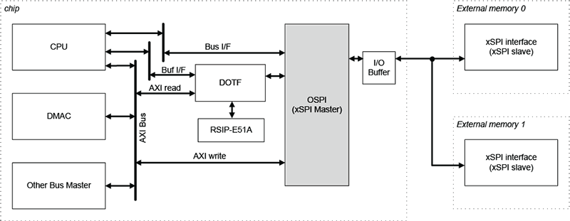
Figure 2. Octal SPI supporting DOTF
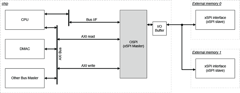
Figure 3. Octal SPI not supporting DOTF
Some features of the Octal SPI interface:
▪ Protocol – xSPI, compliant with
– JEDEC standard JESD251 (Profile 1.0 and 2.0)
– JESD251-1 and JESD252
▪ Supported memory types – octal flash and octal RAM, HyperFlash, and HyperRAM
▪ Data throughput – up to 200MB per second
▪ Data transmission/reception – can communicate with up to 2 slaves using chip select, rather than concurrently
▪ Support for execute-in-place (XiP) operations
▪ Supported modes
– 1/4/8 pin (1S-1S-1S, 4S-4D-4D, 8D-8D-8D) with SDR/DDR
– 2/4 pin with SDR (1S-2S-2S, 2S-2S-2S, 1S-4S-4S, 4S-4S-4S)
▪ Memory mapping
– Each CS supports up to 256MB address space
– Prefetch capability for low-latency burst reads
– Excellent buffering for high-throughput burst writes
▪ Security – supports DOTF (available on some RA8 MCUs)
In addition to internal flash and external memory interfaces, RA8 MCUs also include tightly coupled memory (TCM) and I/D caches that help optimize performance. TCM is zero-wait state memory with the lowest latency among all on-chip memory; it can be used for the most critical parts of the code.
With the various memory and memory interfaces available on RA8 series MCUs, a variety of flexible memory configurations can be achieved. Code can be stored in internal embedded flash and executed from internal embedded flash, resulting in simple, low-latency, highly secure, and energy-efficient systems. However, this is not a scalable solution, as any increase in code size beyond the embedded flash size needs to be addressed through external memory.
In the second configuration, code is stored in external flash and executed from external flash. This is the XiP functionality and is the most flexible and scalable option. As code size increases, external memory can simply be replaced with pin-compatible, higher-density devices without the need to redesign the PCB, making upgrades easy. This comes at the cost of slightly higher power consumption and greater latency, which may impact overall performance.
Code can also be stored in external flash and imported into internal SRAM or TCM for execution. This provides the highest performance as the code is executed through fast SRAM, but there are limitations on code size based on SRAM size; if the code size exceeds the available SRAM or TCM, it increases software complexity. Wake-up time may also increase as code lost when SRAM is off needs to be reloaded at every restart.
Conclusion
There is no single right answer when it comes to choosing memory options. While most mid-to-low-end IoT applications can use internal flash, many high-performance applications require external flash. Memory selection must be based on several considerations – application requirements, required memory size, expected performance, system architecture, power consumption targets, security issues, and future product/platform plans, etc.
Both options have their advantages and disadvantages:
|
Internal Flash |
External Flash |
|
Provides simplicity |
Flexibility |
|
Tightly integrated |
Internal expansion |
|
Highly secure solution |
Scalability |
|
Suitable for a wide range of applications |
Very suitable for emerging IoT and edge AI applications |
By understanding these trade-offs, developers can make informed decisions that align with their project goals.
Get all the details on the flexible memory options available on the RA8 MCU series on each device product page, along with datasheets, samples, and evaluation kits.
For more information, you can identify the QR code below or copy the link to open in your browser:
RA8 MCU Series
https://www.renesas.cn/zh/products/microcontrollers-microprocessors/ra-cortex-m-mcus/product-selector?parametric_selections=25456556%2C25566640%2C25566642%2C25447396%2C25463106
RA8E1 Product Group User Manual
https://www.renesas.cn/zh/document/mah/ra8e1-group-users-manual-hardware?r=25567675
RA8M1 Product Group User Manual
https://www.renesas.cn/zh/document/mah/ra8m1-group-users-manual-hardware?r=25567675
———— END ————
CoreMark Source Code Tutorial Ported Based on RA Microcontroller
Renesas RA8 Series Tutorial | Implementing RTC Real-Time Clock Function Based on e2s

General Methods for MCU Code Self-Check and Diagnosis