Welcome FPGA engineers to join the official WeChat technical group.
Clickthe blue textto follow us at FPGA Home – the best and largest pure FPGA engineer community in China

Recently, I have been working on ARM-related studies and feel it is necessary to document my previous work on FPGA; a good memory is not as good as a bad pen. Speaking of FPGA, I have been using it intermittently for 4 to 5 years, and I have almost forgotten everything due to the lack of documentation. My insights on FPGA will be summarized from the following aspects:
1. FPGA timing constraints and high-speed ADC constraint examples
2. TDC carry delay chain design and research
3. TDC accuracy and implementation of automatic calibration algorithms
STA: Static Timing Analysis
The importance of STA (Static Timing Analysis) in the actual FPGA design process is self-evident. Its role is:
1. To help analyze and verify whether an FPGA design’s timing meets the requirements;
2. To guide the fitter (routing synthesizer) to layout and route to meet the required results;
In simple terms, static timing analysis (STA) tells us how the circuit actually performs, while providing constraints (SDC files, i.e., the requirements above) to inform the analysis tools how we want the circuit to perform. The STA tool TimeQuest TA that comes with Quartus II is used in the FPGA design process as shown in the figure below:
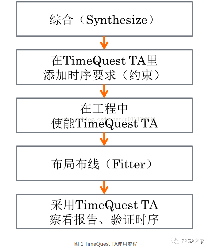
Figure 1 TimeQuest TA usage flow
In short, we need to learn:
A. Correctly understand timing; see background knowledge introduction
B. Correctly write SDC files and use TimeQuest TA to generate SDC constraint commands; SDC introduction
C. Use TimeQuest TA to view and verify timing
1. Background knowledge introduction:
1.1 Launch edge and latch edge:
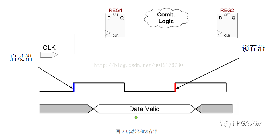
Figure 2 Launch edge and latch edge
Launch edge: The clock edge at which data is launched; in other words, each launch edge generally produces new data!
Latch edge: The clock edge at which data is latched; in other words, each latch edge saves new data!
For the cascaded register circuit shown in the figure above (ignoring the logical relationship between the output of the previous flip-flop and the input of the next flip-flop), the blue rising edge generally serves as the launch edge for the first flip-flop, while the red rising edge (which usually follows the launch edge) serves as the valid edge. Therefore, after the blue launch edge, valid data is output from REG1 and latched into REG2 at the red edge and output to the next stage.
1.2 Setup and hold times

Figure 3 Setup and hold times
The above latch edge will save the data, but certain conditions must be met:
Setup time Tsu: The minimum time for data to remain stable before the clock valid edge;
Hold time Th: The minimum time for data to remain stable after the clock valid edge;
This is akin to a window of time during which the data must remain stable within the valid edge window; the timing of the clock signal and the timing of the data signal are both the timing actually perceived by the registers; what is actually perceived will be analyzed further below;
1.3 Data arrival time (DAT)
All signals propagate within the FPGA with delays, including clock signals and data signals (in reality, these two types of signals should not be distinguished, as under certain conditions, these two signals may be interchangeable, but that is another topic). This means that there will be a delay from the signal’s point of emission to its point of reception, which may be due to the internal spatial distribution of the FPGA or may be caused by combinational logic; this will not be explored further here;
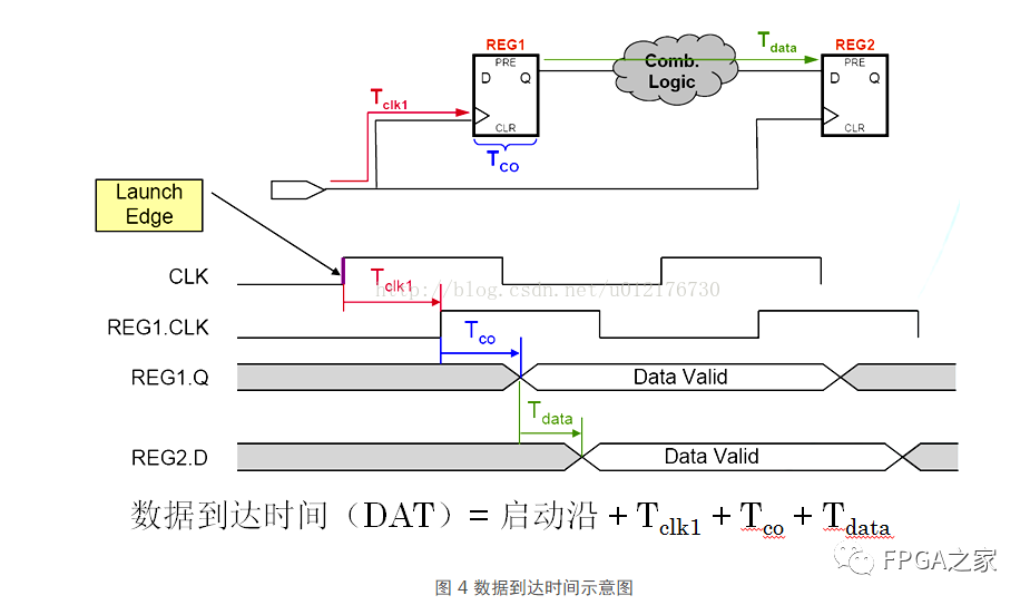
Figure 4 Data arrival time illustration
As shown in the figure above, when calculating the data arrival time, there are generally three delays:
1. Tclk1: The time taken for the clock signal to reach the corresponding clk port of the launch register (or launch flip-flop) from its starting point (usually the PLL output or the clock input pin); if CLK is the clock signal output from the PLL (referred to as the source clock), this signal travels through the FPGA’s internal “wiring” and eventually reaches REG1’s clk port, so at this time there will also be a periodic clock signal REG1.CLK at REG’s clk1 (as shown in the figure); it can be seen that at this time, CLK (source clock) and REG1.CLK actually have a (phase difference) time difference, and this time difference is Tclk1;
2. Tco: The internal delay of the launch register, which is the delay from when the register REG1 perceives the valid rising edge to when the data actually outputs from REG1’s Q; please note that the aforementioned effective rising edge refers to REG1.CLK, not CLK; thus, the actual timing of valid data output is as shown in REG1.Q in the figure;
3. Tdata: The delay from the output Q of the upper register (after passing through all other combinational logic and internal FPGA wiring) to the data input D of the lower register; as shown in the figure, data flows from REG1’s Q to REG2’s D, so the data timing actually perceived by REG2 is REG2.D;
If the launch edge in the figure is set as time zero, the sum of the series of delays is referred to as data arrival time, DAT:
DAT = Launch edge + Tclk1 + Tco + Tdata;
1.4 Data require time (setup) (DRTsu)
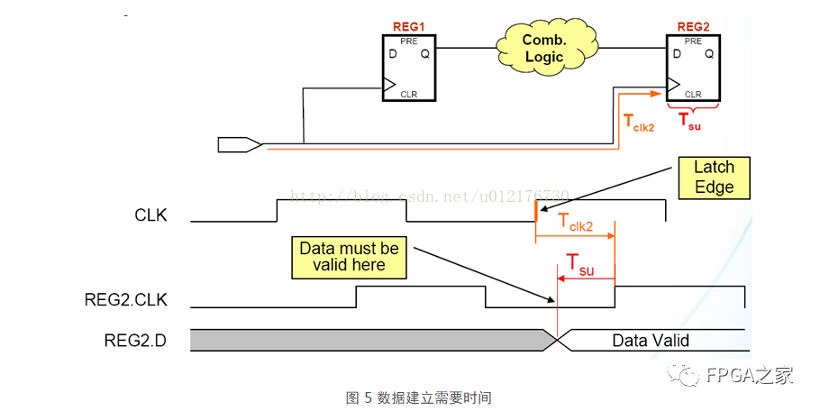
Figure 5 Data require time (setup)
Using the same analysis method, the data setup time also requires two delays:
1. Tclk2, which differs from Tclk1 mentioned above; this delay is the time taken for the clock to travel from its starting point (usually the PLL or clock input pin) to the latch flip-flop; as shown in the figure, REG2 actually perceives the clock from its own clk pin, not the source clock CLK, and there exists a delay between them, which is Tclk2; thus, the clock perceived by REG2 is actually REG2.CLK in the figure;
2. Tsu: As analyzed earlier, every piece of data being latched must meet the setup and hold time requirements, Tsu is the setup time, meaning that when REG2 actually perceives the Latch Edge, the data must arrive at REG2’s D Tsu time in advance to be correctly latched;
Combining the clock wiring delay Tclk2 and Tsu, we obtain the data require time DRTsu:
DRTsu = Latch edge + Tclk2 – Tsu.
This means that the data must be valid and stable before the DRTsu time.
1.5 Data require time (hold) (DRTh)
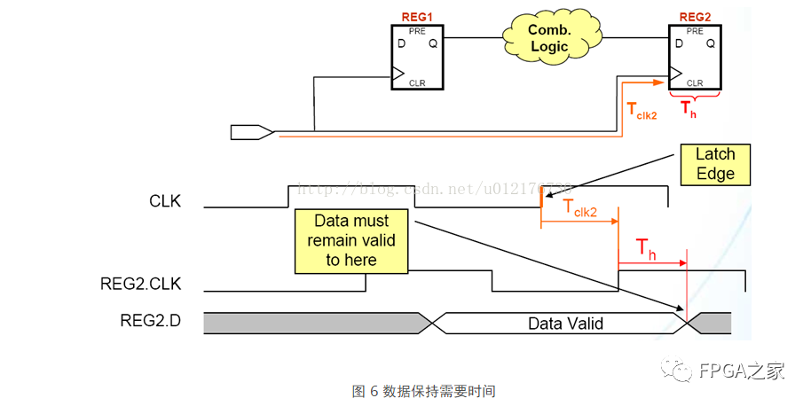
Figure 6 Data require time (hold)
That is, DRTh = Latch edge + Tclk2 + Th;
This means that the data must remain unchanged before the DRTh time;
1.6 Setup slack
Setup slack refers to the relationship between data arrival time and data require time:
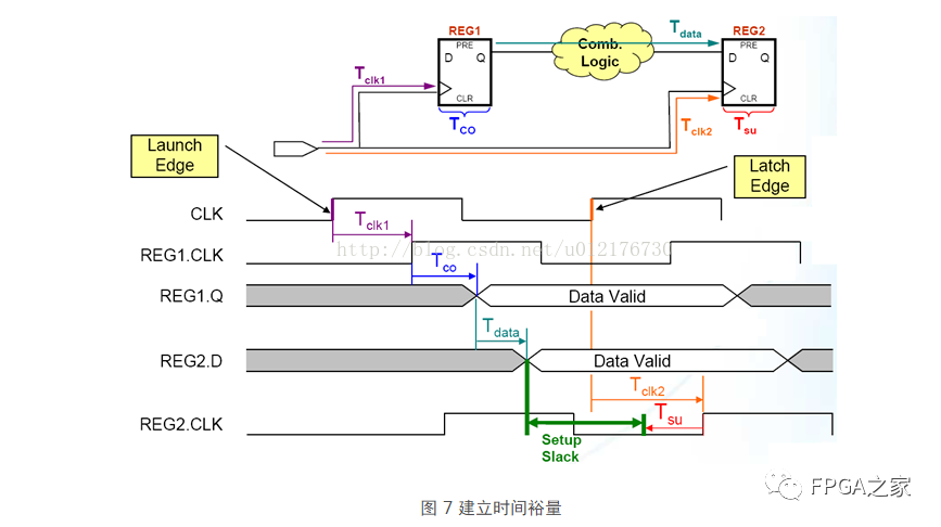
Figure 7 Setup slack
As shown in the figure above, at time zero (Launch edge), the source clock CLK says, “Ah, I want to generate new data,” but this command (launch edge) does not immediately reach REG1; instead, there is a delay of Tclk1. Therefore, at time Tclk1, REG1 finally hears (perceives the effective clock rising edge, which is the launch edge) the command from the boss and begins to prepare; it waits a moment, then delays Tco, and finally produces data (valid data appears on REG1.Q); this valid data also slowly reaches its destination, wasting Tdata. Ultimately, after Tclk1 + Tco + Tdata time, REG2 receives this data; do not think that REG2 receiving this data is the end of the story; REG2 is also a proud child, and how it is proud will be analyzed further. After the boss CLK sends the launch edge at time zero, it rests for a clock cycle, and at the Latch edge, it suddenly remembers that REG2 must receive the data sent out by REG1; otherwise, it will be wasted. Thus, it issues a command to REG2 that new data is coming, prepare to receive! However, this command does not arrive at REG2’s ears immediately, but takes Tclk2 time. By the time REG2 receives the command (actually perceives the effective Latch Edge), it checks if there is data already at its doorstep (checks if REG2.D has data) and also checks if this data meets its requirements (satisfies the latching conditions); it requires that the data must have waited Tsu time when it received the boss’s command (data setup time), and must also hold for Th time (data hold time). If all conditions are met, REG2 happily accepts this data; otherwise, it will think that REG1’s prepared data is too lazy (did not arrive early by Tsu time) or too impatient (did not linger for Th), and will refuse to accept it!
Therefore, there are two requirements here: the first is the setup slack:
As shown in the figure above, Setup Slack = DRTsu – DAT.
If Setup Slack is positive, it indicates that the data reached the target within the specified time. Conversely, if it is negative, it indicates that the data did not reach the target within the specified time, and the data latched by REG2 is likely to be in a metastable state;
1.7 Hold slack
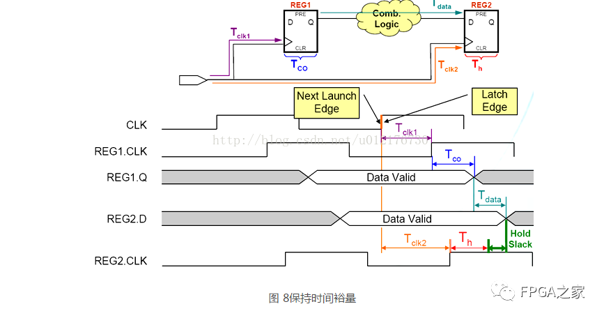
Figure 8 Hold slack
As described above, hold slack = DAT – DRTh
If it is positive, it indicates that there was enough stable time when the data was latched and is valid. Conversely, it indicates that the data is incorrect or may be in a metastable state;
Summary:
Understanding the above seven concepts clarifies that if the clock frequency is too fast or the data delay is too large, it will lead to incorrect timing. All delays between internal registers in the FPGA are based on timing models, such as slow and fast; these models analyze whether the FPGA can work normally under two extreme operating conditions. As long as these two working conditions are met, the FPGA can meet timing in other environments!

Welcome FPGA engineering and embedded engineers to follow our public account.

National Largest FPGA WeChat Technical Group
Welcome everyone to join the national FPGA WeChat technical group. This group has thousands of engineers, a group of technology-loving engineers, where FPGA engineers help and share with each other, creating a rich technical atmosphere! Hurry up and invite your friends to join!!

Press and hold to join the national FPGA technical group.
FPGA Home Components Chip City
Advantageous component services, please scan the code to contact the group owner: Jin Juan Email: [email protected] Welcome to recommend to procurement
ACTEL, AD part of advantageous ordering (operating the full series):
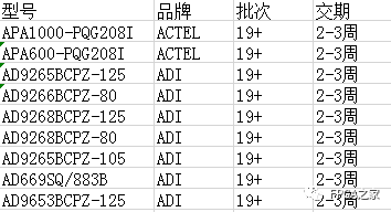
XILINX, ALTERA advantageous in-stock or ordering (operating the full series):
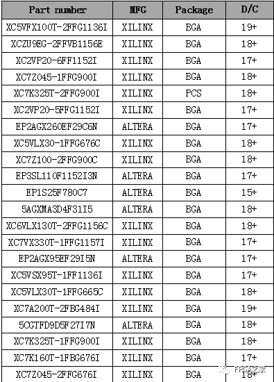
(The above devices are part of the models; for more models, please consult the group owner Jin Juan)
Service concept: FPGA Home Components self-operated Chip City aims to facilitate engineers in quickly and conveniently purchasing component services. After years of dedicated service, our customer service covers large publicly listed companies, military scientific research units, and small and medium enterprises. Our greatest advantage is emphasizing the service-first concept and achieving fast delivery at competitive prices!
Directly operated brands: Xilinx ALTERA ADI TI NXP ST E2V, Micron, and over a hundred component brands, especially adept at handling components subject to US export restrictions against China.We welcome engineer friends to recommend us to procurement or consult us personally!We will continue to provide the best service in the industry!

Official thanks to brands in the FPGA technical group: Xilinx, Intel (Altera), Microsemi (Actel), Lattice, Vantis, Quicklogic, Lucent, etc.