FPGA has various configuration modes: the parallel master mode involves one FPGA and one EPROM; the master-slave mode supports programming multiple FPGAs with one PROM; the serial mode can use serial PROM to program the FPGA; and the peripheral mode allows the FPGA to be programmed by a microprocessor as a peripheral device.
How to achieve fast timing convergence, reduce power consumption and costs, optimize clock management, and lower the complexity of parallel design between FPGA and PCB has always been key considerations for system design engineers using FPGAs. Nowadays, as FPGAs evolve towards higher density, larger capacity, lower power consumption, and more integrated IP, system design engineers benefit from these excellent performances while also facing new design challenges brought about by the unprecedented performance and capability levels of FPGAs.
In many project designs, Altera’s Cyclone series devices based on SRAM architecture are used. Like other FPGA devices, Cyclone devices provide programmable resources based on a gate array method, with their internal logic structure determined by configuration data. This configuration data can be loaded into the internal SRAM of the FPGA through various modes. Due to the volatility of SRAM, the FPGA must be reconfigured each time it is powered on.
1 Cyclone FPGA Configuration Modes
The Cyclone series FPGA devices mainly have three configuration schemes: active serial (AS) configuration using low-cost configuration chips, passive serial (PS) configuration, and JTAG-based configuration. In practical applications, one of these schemes can be used to configure Cyclone series FPGA devices to achieve the desired user programming functions.
Cyclone series FPGA devices use SRAM cells for configuration data. Since SRAM data is easily lost when powered off, the configuration data must be downloaded immediately to the powered Cyclone device. Different configuration modes can utilize different dedicated configuration chips or data sources.
These three configuration modes are determined by the high and low levels of the mode selection pins MSEL1 and MSEL0 of the Cyclone device. If your application requires only a single configuration mode, you can connect the mode selection pins to the VCC or ground. During the switching of pins, the operational state of the device will not be affected. In any case, the levels of the mode selection pins must be valid before reconfiguration.
2 Active Serial (AS) Configuration with Configuration Chips
In AS configuration mode, new low-cost devices (such as EPCS1, EPCS4) are utilized. This dedicated configuration chip has a permanent memory and a simple four-pin interface. Due to its low cost, it can solve the problem of high-cost configuration devices. The serial configuration chip provides a serial interface to access data. During configuration, the Cyclone FPGA reads data through the serial interface, decompresses the data if necessary, and configures the SRAM cells of the FPGA. This mode is controlled by the FPGA, and this scheme is referred to as active serial configuration, abbreviated as AS configuration. The schematic diagram for configuring a Cyclone FPGA device in AS mode is shown below.
The dedicated serial configuration chips can be either EPCS1 or EPCS4, where EPCS1 has a storage capacity of 1Mbits and EPCS4 has a storage capacity of 4Mbits. Designers can choose based on the size of the configuration file. The main configuration pins for the active serial configuration chip are:
DCLK, the serial clock input from the Cyclone FPGA device, provides the clock for the serial interface; DATA, the serial data output, reads data on the falling edge of DCLK; ASDI, the control signal input, latches data on the rising edge of DCLK; nCS, the enable input, is active low.
During system power-up, both chips enter the power-on reset phase. Once in power-on reset, the nSTATUS pin is low, indicating it is resetting; at the same time, the CONF_DONE pin is low, indicating the chip has not yet been configured. After a reset delay of 100ms, the FPGA releases the nSTATUS pin, which becomes high due to the pull-up resistor, and enters the configuration state. Once the reset is exited, all user I/O pins enter a tri-state condition. The clock signal DCLK is generated internally by the FPGA to control the entire configuration cycle and provide the clock for the configuration chip’s serial circuit, with a frequency range between 14MHZ and 20MHZ. When the DCLK falling edge arrives, the FPGA outputs control signals and allows the configuration chip to output configuration data; when the DCLK rising edge arrives, the FPGA latches the configuration data and the configuration chip latches the control signals. After all configuration data is received, the FPGA releases the CONF_DONE pin, which is pulled high by a 10K pull-up resistor, and begins to enter the initialization phase. The Cyclone FPGA device requires 136 clock cycles for strict initialization. Then it enters the user state, at which point the INIT_DONE pin transitions to high.
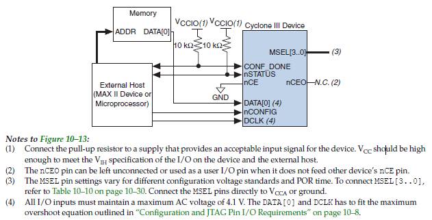
3 Passive Serial (PS) Configuration Based on Microcontrollers
A simplified circuit diagram of the passive serial configuration scheme for Cyclone FPGA using a microprocessor. The microcontroller configuration process is simple; it only needs to connect 5 I/O ports to the FPGA. These 5 signal lines are: DATA0, DCLK, nCONFIG, nSTATUS, and CONF_DONE.
The specific configuration process is as follows: ① nCONFIG=0, DCLK=0, hold for more than 2us; ② Check nSTATUS; if it is 0, it indicates that the FPGA has responded to the configuration request, and configuration can begin; otherwise, report an error. Normally, nSTATUS will be 0 within 1us after nCONFIG=0; ③ nCONFIG=0, wait for 5us; ④ Place data on DATA0, DCLK=1, delay; ⑤ DCLK=0, check nSTATUS; if it is 0, report an error and restart; ⑥ Prepare the next bit of data and repeat (4) and (5) until all data is sent; ⑦ At this point, CONF_DONE should change to 1, indicating that the FPGA configuration is complete. If CONF_DONE is not 1 after all data is sent, reconfiguration is necessary; ⑧ After configuration is complete, send several cycles of DCLK to allow the FPGA to complete initialization.
It is worth noting that SOF or POF files generated by MAX+PlusⅡ or QuartusⅡ cannot be directly used for microcontroller configuration of the FPGA; data conversion is required to obtain usable configuration data. In MAX+PlusⅡ or QuartusⅡ, there are options for data conversion, converting .SOF files to .rbf files, which can then be directly written into a specific ROM or Flash area of the microcontroller system. The starting address and length of this data are known, and corresponding software can be written according to the above process.
4 Configuration Data Compression Methods
Cyclone devices are FPGA devices that support decompression of configuration data, allowing configuration data stored in configuration chips or other memories to be compressed. During configuration, this compressed data is sent to the Cyclone device, decompressed in real-time, and used to program the SRAM cells. Both AS and PS configuration modes support compression, while the JTAG-based configuration mode does not support compression. Preliminary data indicates that compression can reduce the configuration data bitstream by 35% to 60%, reducing storage space and transmission speed as well as the cost of configuration devices.
QuartusⅡ can generate configuration files with compression, reducing the space of configuration chips and flash memory, as well as the transmission time of bitstreams. Below, we will introduce two methods for operating compressed configuration files using QuartusⅡ version 5.1 as an example.
4.1 Method 1: Activate compression in project settings before writing the design program.
First, click on the Device item under the Assignments menu to pop up the Settings window. Then select Cyclone devices in the Family option, click on the Device & Pin Options window below, choose the Configuration window, click on the Generate Compressed bitstreams option, and finally press the OK button to complete the settings.
4.2 Method 2: Activate compression from the Convert Programming Files window after writing the design program.
First, pull down the File menu, click on Convert Programming Files to pop up the window, select the file type Programming File type (POF, SRAM HEXOUT, RBF, or TTF), then for POF output files, select the configuration device, choose Add File to add a Cyclone SOF file, select the filename to add to the SOF Data area, click on the Properties option, then OK, and finally press the Generate button to create.
5 Conclusion
The serial configuration method has a simple hardware circuit, the configuration process is easily implemented in software, and it is convenient for engineering applications. The logic resources and chip speed of Cyclone series FPGA devices can meet project requirements, providing high cost-performance ratios and certain expandability. This FPGA configuration implementation method is also applicable in conjunction with other CPUs for various applications, as long as the hardware and software configuration requirements are strictly followed, making it of reference value in practical applications. Nowadays, CPLD/FPGA has become a platform for digital system development, and in the future, it will continue to improve and enhance towards high integration, large capacity, low cost, low voltage, low power consumption, diverse resources, suitability for system-on-chip (SOC), deep sub-micron processes, various soft and hard IP libraries, and practical dynamic reconfiguration technology.