The deployment of Internet of Things (IoT) technology has started to make tangible progress. The potential scale and diversity of the market are driving significant innovations, with new technological advancements and emerging communication protocols propelling IoT towards the projected billions of nodes in the coming years.
Engineers may have extensive expertise in their specific functional areas, but they may feel challenged when facing unfamiliar IoT hardware and software design and development issues. As this situation becomes more common, engineers need node-to-cloud platforms like ON Semiconductor’s versatile IoT Development Kit (IDK), which have proven to accelerate and simplify the deployment of IoT functionalities across various design fields.
With a wide array of connectivity, sensing, and actuation options available for designers, developing IoT solutions has become more complex. If a prototyping platform can evaluate multiple energy efficiency options and quickly prototype an end-to-end solution, it would significantly shorten product development and deployment times. Platforms like IDK, which offer various connectivity, sensing, and actuation options, provide design flexibility that is crucial during the evaluation and prototyping phases.
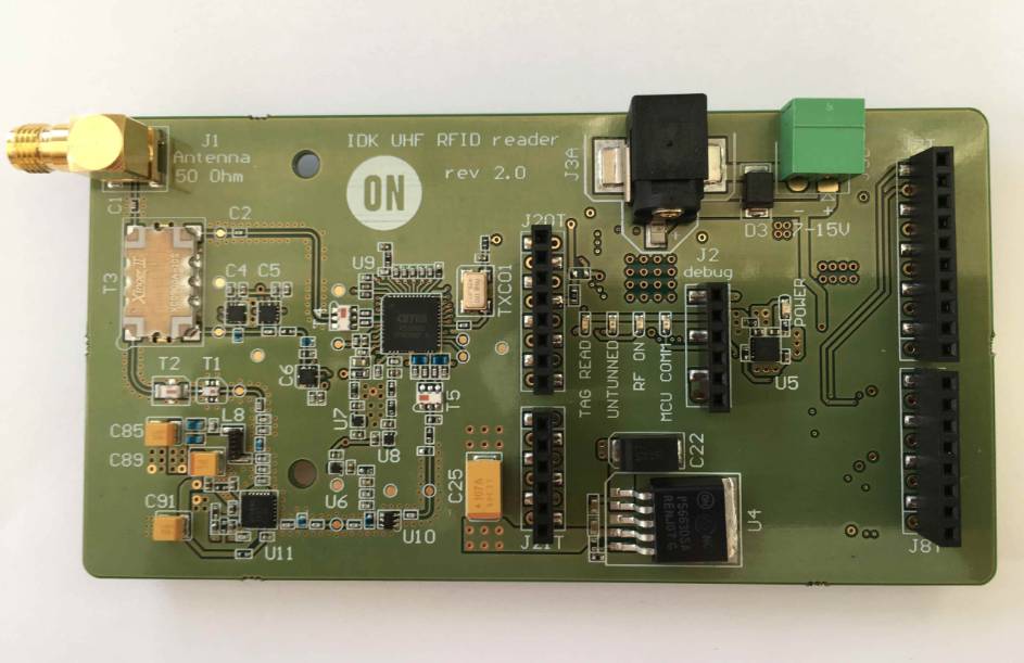
ON Semiconductor’s IDK recently added two new shield boards (sub-boards) for Bluetooth Low Energy wireless connectivity and for reading temperature, pressure, and humidity data from the company’s battery-free energy harvesting sensors.
The new shield boards bring a whole new customer layer to the IDK, enabling unique types of IoT applications. Energy harvesting and battery-free sensing technologies are pioneering a whole new paradigm of IoT use cases in areas such as industrial quality control, predictive maintenance, health monitoring, and agriculture. Meanwhile, ubiquitous Bluetooth Low Energy technology creates wireless connectivity possibilities with minimal impact on battery life—an essential requirement for many IoT implementations.
The newly released shield boards, along with existing sensing, actuation, and connectivity options, significantly expand the applications that can be built on the IDK. Furthermore, using ultra-low-power devices on the IDK allows designers to create IoT products with longer battery life.
The hardware products of the IDK are complemented by an Eclipse-based integrated development environment (IDE) with an intuitive user interface. The IDE also provides various application programming interfaces (APIs) and use cases for verticals such as smart homes/buildings, predictive maintenance, and wearable/mobile healthcare. The software framework also includes a C++ compiler, debugger, code editor, and several application-related libraries.
The IDK also includes design schematics, PCB layouts, and photoplot files, further accelerating the rapid transition from concept and development to production, allowing terminal product design to be completed almost entirely via a “copy-paste” method.
↓↓↓ Read the original article for more!