Author Introduction
Dr. Liu, Ph.D. from University of Electronic Science and Technology, an expert in microarchitecture.
1. Background
The clock circuit is the most basic circuit in the chip. The performance of the clock circuit is related to whether all the modules in the SoC can achieve the expected goals, such as the main frequency of the computing core (CPU/GPU/NPU), the bandwidth of DDR, the bandwidth of high-speed interface (PCIE), etc. For the clock circuit, the most critical performance metric is the jitter, which will affect the frequency of the digital circuit and the bit error rate of the SerDes. Therefore, it is particularly important to reasonably consider the clock jitter of each module in the early stage of design.
For automotive chips, there are higher requirements for jitter because they need to have the safety mechanisms to detect faults. ISO26262 has clearly defined the automotive safety integrity level (ASIL), which are ASIL A, ASIL B, ASIL C, and ASIL D from low to high. The corresponding single-point fault rate is shown in Table 1.

Table 1. Possible source for the derivation of the target “single-point fault metric” value
At the same time, due to the increasing demand for computing power for cockpit and ADS chips, the chip area and power consumption are also increasing. Larger area and higher power consumption bring great challenges to the clock design of the chip: the long-distance clock path and power supply noise will significantly deteriorate the clock jitter, which will deteriorate the performance of the entire chip. Therefore, it is particularly important to analyze the effect of various jitters on chip performance and then to fine-tune the chip design.
No real clock sources in the real physical world (PLL’s, DLL’s, Crystal Oscillators, even function generators) exist that have a single, fixed value for their output period. The output period of all real clock sources changes over time. The exact placement of clock edges will vary both within a clock period and from one clock period to the next. This variance in period is known as jitter.
This article explains some of the key terminology and parameters commonly used to describe jitter. It will also help clarify the most important parameters for some PLL applications, allowing the designer to better understand what is required from a PLL.
2. Applications
Different applications have different requirements for jitters.
2.1 Digital Systems
In a digital system, the clock defines a period during which the circuits can achieve a certain amount of work. Since each sub-unit of work (logic gate intrinsic delay, rise/fall transition delay, wire delay, etc.) takes a certain period to complete, then the overall frequency (period) of the system is a major constraint on logic complexity and allowed logic depth in synchronous digital systems.
In digital systems, clock edges define the time at which each work unit starts and ends. When jitter changes edge timing to reduce the length of an individual clock cycle, it reduces the amount of time available for the unit of work to complete.
Period jitter is a measure of how individual clock cycles vary and hence is the best indicator of how much time is available for each unit of work. This is the primary characteristic that digital systems designers should focus on and closely specify.
2.2 RF Systems
The Local Oscillator (LO) for an RF system defines the carrier frequency and is generally used in the mixers used to generate the transmitted signal and down-convert the received signal for processing.
In this context, accumulated jitter (long-term jitter) is a measure of the total phase noise in the system. When a signal is multiplied by a clock to up-convert or down-convert, the resulting spectrum becomes the multiplication of the spectrum of the signal with the spectrum of the clock. Any phase noise in the clock signal will result in an undesired signal at the output, reducing the signal-to-noise ratio (SNR) of the system.
2.3 ADC/DAC
In Analog to Digital Converters (ADC) and Digital to Analog Converters (DAC), the clock sets the time at which the sample is taken. If the signal is changing with time and jitter causes the sampling time to change from the ideal instant, this will result in a change in the sampled value of the signal versus an ideal reference sample value.
The sampling of an ADC or DAC can be modeled as a multiplication of the signal with the clock. This means that the SNR of such a system is degraded in exactly the same way as described in Section 2.2, and accumulated jitter is again the important parameter.
2.4 SerDes Systems
When transmitting or receiving a serial bit stream, using a SerDes or similar, the clock is used to encode and time the transmitted data, embedding clock information within the transmitted data itself. Separately the receiver has its own clock, derived from the received data, to sample and capture the data. In this system, accumulated jitter is important as this sets the difference in time between when a bit arrives and when that bit is sampled. If the jitter of this combined system is too big, then the wrong bit value will be sampled.
3. Random and Deterministic Jitter
When measuring jitter, it is important to consider the behavior across many cycles to see what the aggregate performance will be in a statistical sense. For RF Systems, ADCs and DACs, this statistical data generates the important information that the system designer needs directly. Whilst for digital systems, it gives the probability that a clock cycle will be shorter than the target cycle time, which is the key metric for timing closure.
3.1 Random Jitter
The jitter generated within a PLL is primarily band-limited random jitter. In addition, white noise on the PLL supplies can be translated into random jitter at the PLL output.
Random jitter comes from processes that are truly random such as thermal noise and flicker noise. Random jitter may also result from power supply noise, where that noise in turn originates from random processes, such as thermal noise, in the circuit supplying power to the SoC and to the PLL.
Random jitter, as its name suggests, cannot be predicted accurately for any given cycle. Only the statistical properties of a set of clock cycles can be estimated. The most useful measure of random jitter is the standard deviation of the random distribution, which is the same as the RMS jitter.
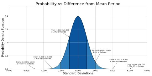
Figure 1. Normal Distribution
Figure 1 shows the normal distribution, typically used to model jitter probability. All random jitter from a PLL follows a normal distribution.
For each whole standard deviation (σ) from 1 to 6, the probability of a clock edge being outside that number of σ from the mean is annotated on Figure 1. It can be seen that this approaches zero very quickly, but never reaches zero. For example, there is a 31.7% chance that a clock edge is more than 1σ from the mean, but the probability that it is more than 6σ from the mean is 1.97×10⁻⁹, a number so small that in almost all analysis cases we can approximate it to zero.
Note that modern digital designs often use more stringent criteria than this, requiring a confidence interval of 5σ or even 6σ. Serial communication standards commonly have even higher requirements and typically specify a larger number of σ that must be used to calculate the peak jitter.
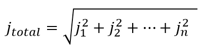
If there are multiple sources of uncorrelated random jitter, they are summed up in an RMS fashion. Thus to get the combined total:
Where:
-
jtotal is the total jitter
-
jk for k=1…n are the individual, uncorrelated jitter components.
3.2 Deterministic Jitter
Deterministic jitter is jitter that follows a known pattern.
Potential sources of deterministic jitter in clock outputs are:
-
Spread Spectrum Clocking (SSC)
-
Deterministic modulation of the power supply: If an SoC has repeating high power and low power modes, this can result in deterministic power supply modulation.
-
Other sources of modulation
-
Any other mechanism that operates in a deterministic manner
The peak deterministic jitter can be measured directly. Because it is deterministic and has no probabilistic dependencies, the measurement is absolute.
For example, the voltage supply to a PLL may exhibit a 500kHz ripple arising from the use of a switched mode power supply. This power supply noise component will result in deterministic period jitter at the PLL output with a measurable peak value which will be proportional to the peak deviation of the input supply. There will be a direct relationship between the power supply voltage at a given time and the instantaneous period jitter of the PLL output clock. As the power supply voltage changes, the change in period at the PLL output will be seen as deterministic jitter.
3.3 Combining Random and Deterministic Jitter
Only the peak or peak-to-peak values of random and deterministic jitter can be combined. To combine these two components:
-
Take the peak value of the random jitter for a given σ (Rj)
-
Take the peak value of the deterministic jitter (Dj)
-
Add the two peak values to calculate total jitter (Tj=Rj+Dj)
4. Jitter Definition and Categories
4.1 Period Jitter
Period jitter is the most important jitter for digital systems. It is the deviation in the period of the clock from the mean period of that clock.
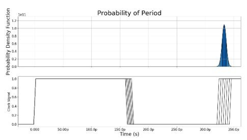
Figure 2. Period Jitter Example
Figure 2 shows an example of period jitter for a 3-GHz clock. Each cycle plotted on the lower axis has a slightly different period from all the others, as shown by the several possible rising edge positions at the end of the cycle. All the rising edges at the beginning of the cycle have been aligned to show the differences in period arising from jitter. There will be some probabilistic distribution of the time of an edge happening, shown here on the upper axis as a normal distribution.
Mathematically, period jitter can be represented as:
jperiod = periodcurrent cycle-periodmean
Where:
-
jperiod is the instantaneous period jitter of a given clock cycle
-
periodcurrent cycle is the instantaneous period of the current clock cycle
-
periodmean is the mean period of the clock being measured
Period jitter consists of both random and deterministic jitter components. These can be analyzed individually, but it is generally unimportant to do so because in most applications where period jitter is important, the only important parameter is the shortest possible cycle.
In a digital system, the shortest possible cycle is the time available for the logic to complete its unit of work.
4.2 Cycle-to-Cycle Jitter
Cycle-to-cycle jitter measures the change between two adjacent clock cycles. This is shown in Figure 3.
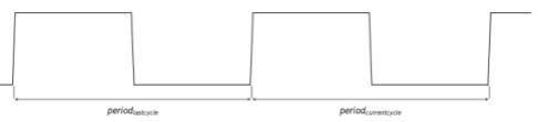
Figure 3. Cycle-to-Cycle Jitter Definition
Mathematically, cycle-to-cycle jitter can be represented as:
jcc = periodcurrent cycle-periodlast cycle
Where:
-
jcc is the instantaneous cycle-to-cycle jitter of a given clock cycle
-
periodcurrent cycle is the instantaneous period of the current clock cycle
-
periodlast cycle is the instantaneous period of the last clock cycle
While commonly discussed in many treatments of jitter, cycle-to-cycle jitter is not generally useful as it does not relate to any commonly used performance criteria in digital, RF, or sampled systems.
4.3 Accumulated Jitter
Accumulated jitter, also known as long-term jitter, is the deviation in the time of a given clock edge from when the same edge of an ideal clock occurs. This can be accumulated over many clock cycles, distinct from period jitter, which only considers a single clock cycle or cycle-to-cycle jitter, which is always measured by two clock cycles adjacent in time.
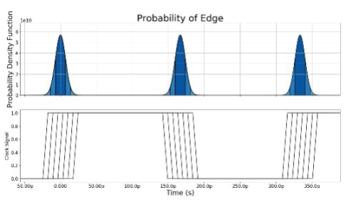
Figure 4. Accumulated Jitter Definition
Figure 4 shows a clock signal illustrating the concept of accumulated jitter.
Accumulated jitter is the accumulation of the period jitter over many cycles. In real systems, we only need to consider the jitter over specific bandwidths, so the accumulated jitter will reach a limit independent of time and will not become infinitely large.
Accumulated jitter is important for the clock of RF systems, ADC/DAC, and SerDes systems. Accumulated jitter is the sum of both random and deterministic components.