Abstract: This article introduces a very old PCB manufacturing process – the etching method. The advantages of this process include low cost and short time. However, there are also significant drawbacks, such as the complexity of making double-sided boards and environmental concerns! The specific manufacturing method is as follows:
Designing the PCB
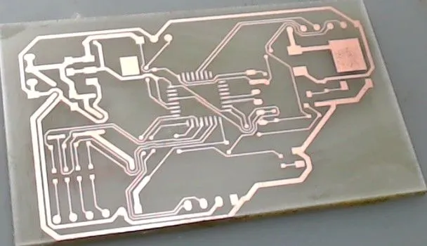
1. Design the PCB using Altium Designer (AD).
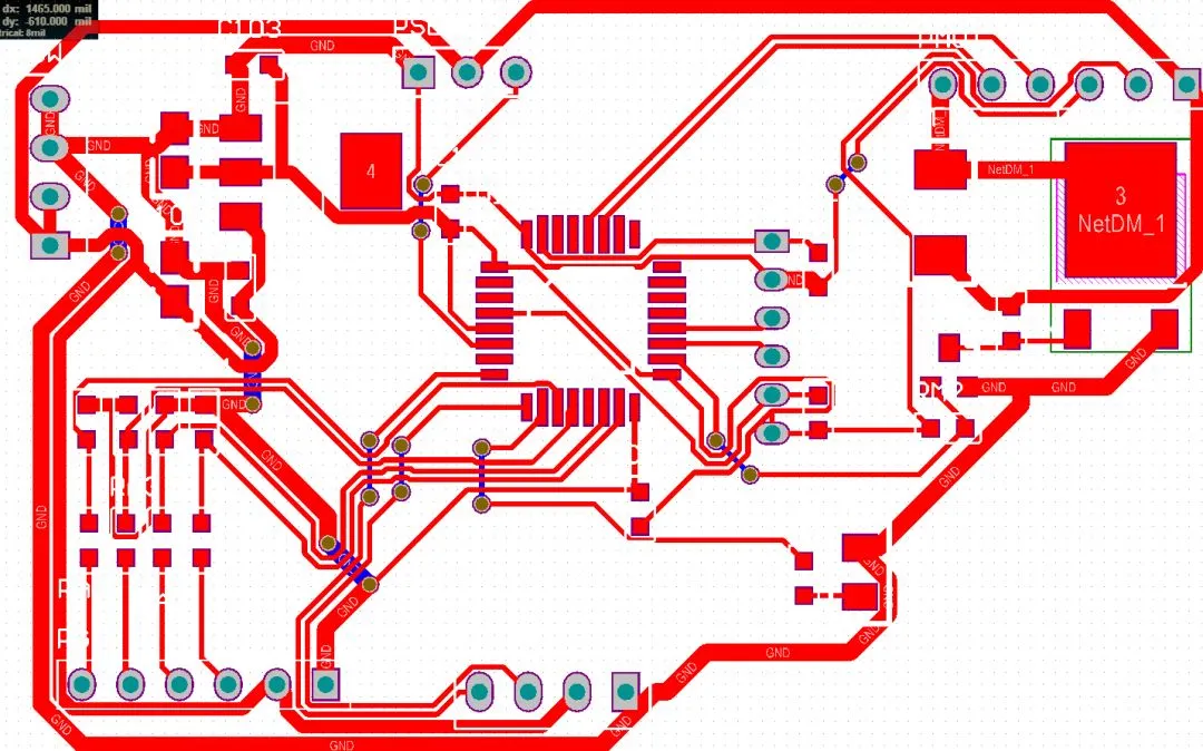
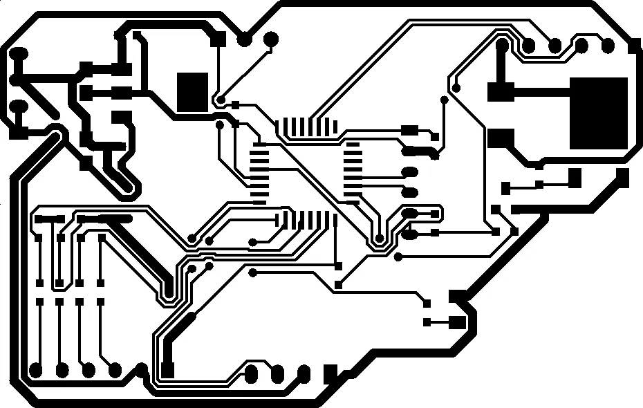
2. Set it to print only the TOP_LAYER and the via layer.
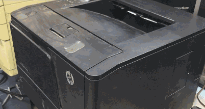
3. Use a laser printer to print on thermal transfer paper.
4. The minimum trace width set for this PCB is 10 mils.
Transferring the PCB Design
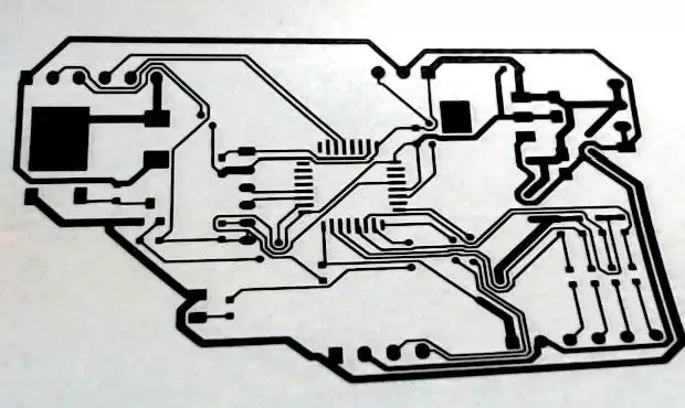
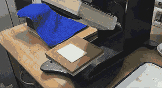
1. Print the black and white electronic circuit design on thermal transfer paper using the laser printer; using oil paper is preferable.
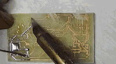
2. For single-sided PCBs, one sheet is sufficient. Attach it to a suitably sized copper-clad board, and under heat and pressure from a thermal transfer machine, the transfer can be completed in 20 seconds. Remove the copper-clad board and peel off the thermal transfer paper to reveal the clear circuit pattern on the copper-clad board.
Etching the PCB
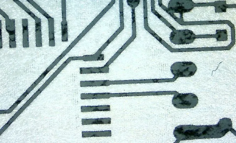
1. Place the copper-clad board in an ultrasonic etching tank, using a mixture of hydrochloric acid and hydrogen peroxide as the etching solution. It only takes 15 seconds to remove the excess copper layer. (This can be replaced with a basin of water, shaken by hand, and the water temperature can be slightly higher to accelerate the etching process. Students with sufficient budget can also buy an etching device online.)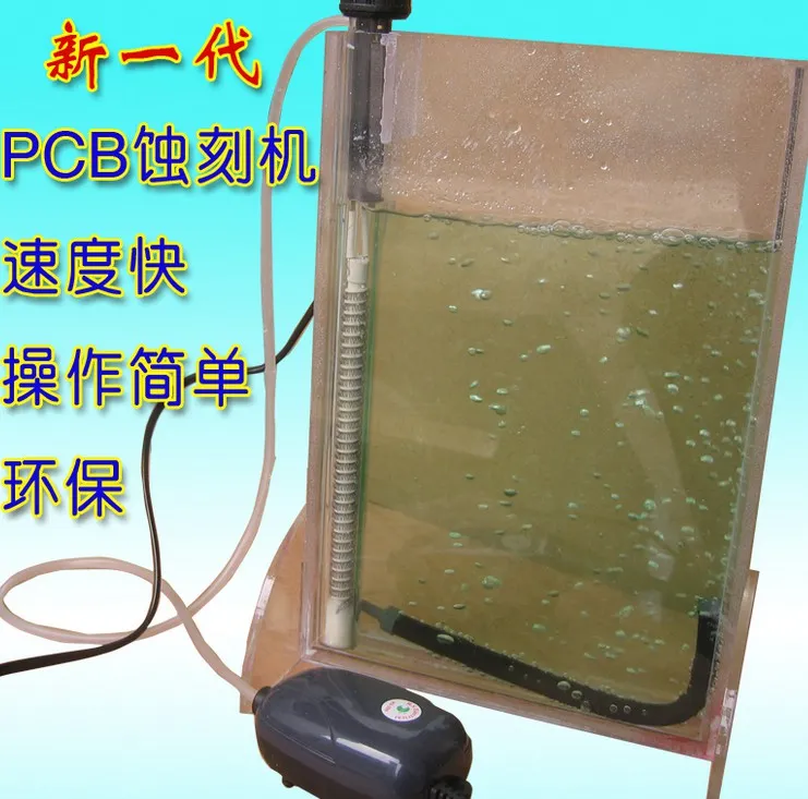 The appropriate ratio of hydrochloric acid and hydrogen peroxide, along with a high-speed ultrasonic etching tank, is key to achieving fast and perfect etching. After rinsing with water, the etched PCB can be removed.
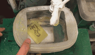
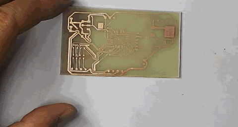
Be very careful not to recklessly touch high-concentration etching solutions. Otherwise, the pain you experience will be a lifelong memory. Be cautious while shaking; in the past, I had several large holes in my pants from making boards. Additionally, do not dispose of the etching wastewater carelessly; previously, there was a lawn in front of the laboratory, and after pouring the etching wastewater, the lawn was dead for several weeks.2. Use acetone or a steel wool ball to wipe off the black toner, and thus a test PCB is completed.
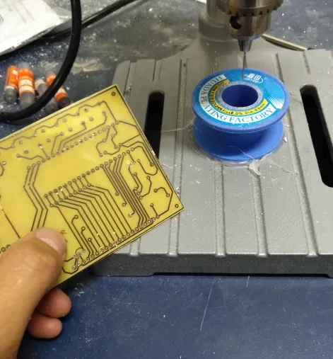
Sometimes, drilling is also required.
Soldering the PCB
1. Apply flux to the surface of the PCB.
2. Use a wide-tipped soldering iron to tin the PCB, making subsequent soldering easier.
3. Remove the flux to complete the soldering of the components.
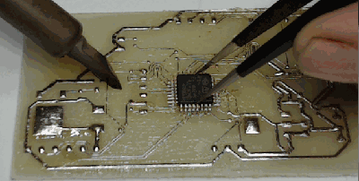
4. Since the solder has been pre-applied, soldering the components is relatively easy.
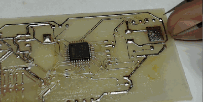
5. After soldering, use board cleaning solution to clean the PCB.
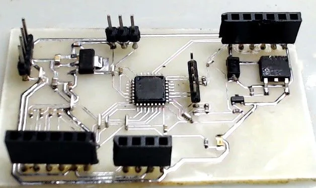
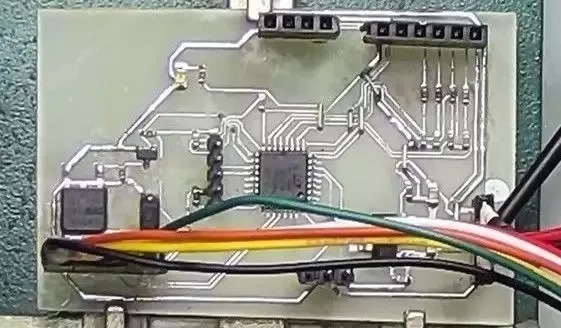
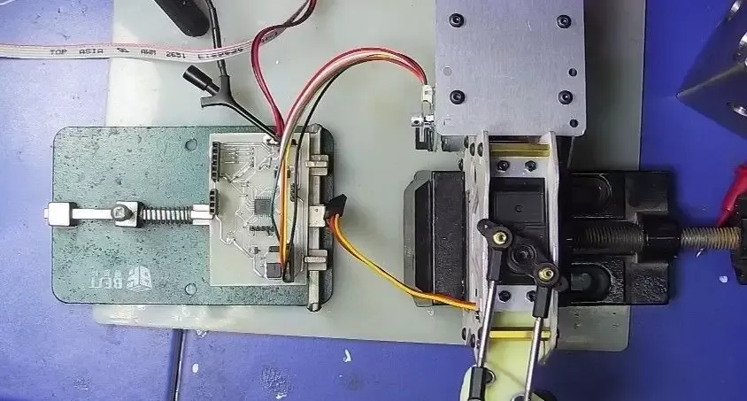
6. The PCB is now in the testing phase.
Source: World Advanced Manufacturing Technology Forum
Disclaimer: This article is copyrighted by the original author and does not represent the views of the association. The articles shared by the “Jiangxi Province Electronic Circuit Industry Association” are for sharing purposes only and do not represent the position of this account. If there are copyright issues, please contact us for removal.