Source: Chip Learning
Original Author: Chip Future
The CH201 is a miniature, ultra-low power, long-range ultrasonic Time-of-Flight (ToF) distance sensor. Based on Chirp’s patented MEMS technology, the CH201 is a packaging system that integrates a PMUT (Piezoelectric Micro-Machined Ultrasonic Transducer) and an ultra-low power SoC (System on Chip), allowing the SoC to run Chirp’s advanced ultrasonic DSP algorithms, including an integrated microcontroller that outputs via I2C digital interface.
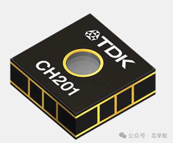
Figure: TDK Ultrasonic Time-of-Flight (ToF) Distance Sensor CH201
The sensor features:
• 3.5mm x 3.5mm x 1.26mm, 8-pin LGA package
• Programmable range from 20 cm to 5 m
• Field of view (FoV) exceeding 180 degrees, capable of detecting multiple targets under any lighting conditions
• A single sensor for both receiving and transmitting
• Maximum range of 5m with power consumption as low as 13.5μA
• Operating frequency of 85kHz
X-RAY non-destructive analysis shows that it contains 2 chips: Chip 1 is the MEMS chip, and Chip 2 is the SoC chip. The MEMS chip faces the package’s front opening to transmit or receive ultrasonic signals, and is electrically connected to the front substrate by two gold wires. The SoC chip is bonded to the bottom substrate and connected electrically through 13 gold wires. The MEMS chip and SoC chip are electrically connected through the package’s vias around the edges.
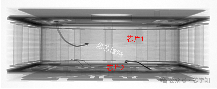
Figure: Front View of CH201
By physically opening the chip, we obtain two parts: the upper substrate contains the MEMS chip, and the lower substrate contains the SoC chip. Each chip is physically bonded to the top and bottom plates using adhesive, and electrically bonded using wire bonding. Vias around the substrate show the electrical connections between the upper and lower plates.
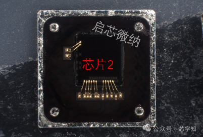
Figure: Opening of CH201
After removing the adhesive from both chips, we extract the core. The piezoelectric MEMS ultrasonic transducer chip in the CH201 is manufactured by STMicroelectronics, with a layout from 2018. STMicroelectronics developed an aluminum nitride (AlN) manufacturing platform to enhance its MEMS integration technology. The SoC chip is a typical IC chip.
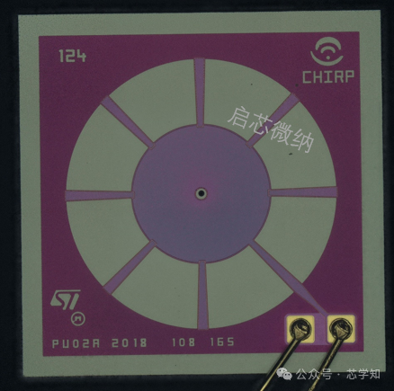
Figure: CH201 MEMS Chip
To analyze the membrane structure of this MEMS chip, we perform a 45° cross-section cut. From the cross-section diagram, we can see the center circular area of the MEMS chip is a membrane structure, i.e., a vibrating membrane structure. The success of this piezoelectric MEMS ultrasonic ToF sensor lies not only in the piezoelectric material but also in the design and manufacturing of the silicon thin film. The physical dimensions, mass, and stiffness of the silicon thin film determine its resonant frequency. All structural designs of this chip are aimed at achieving a good resonant frequency.
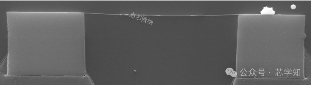
Figure: CH201 Cross-Section Diagram
END
This content is reprinted and represents the author’s views only
It does not represent the position of the Institute of Semiconductors, Chinese Academy of Sciences
Editor: One Two
Responsible Editor: Six Dollar Fish
Submission Email: [email protected]
Previous Recommendations
1. High Purity Silicon Carbide Powder Synthesis Methods
2. The Role and Requirements of PIE in FAB
3. Understanding Femtosecond Laser and Etching Combined Processing Technology
4. Transmission Electron Microscopy Imaging Technology: Coupling in Electron Imaging
5. The Wireless Revolution from Wi-Fi 4 to Wi-Fi 7: A 40x Speed Increase