Understanding OBG in Microcontrollers: The STM32 microcontroller’s core (Cortex-M3) contains a hardware debugging module that supports various complex debugging operations. The hardware debugging module allows the core to halt when fetching addresses or accessing data—this is the assurance we have for online simulation during microcontroller development and debugging.When the core is halted, both its internal and external states can be queried. In microcontroller simulation debugging, interruptions are usually caused by user-set breakpoints. At this point, all variables within the microcontroller, as well as program pointers, CP, and other address pointers, can have their states queried.During debugging, when a breakpoint is set and the program halts, we can continue with single-step execution, step out of functions, enter functions, and other operations.We can also perform a reset to return all registers to their initial reset state.
OBG Debugging Interface
Serial Interface
JTAG Debugging Interface
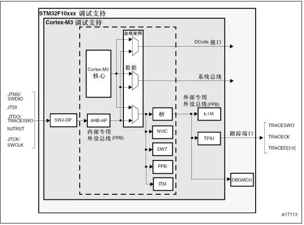
OBG Debugging Block Diagram
SWJ (Serial Wire and JTAG) Debug Port
The JTAG debugging interface (JTAG-DP) provides a 5-pin standard JTAG serial debugging interface, while the SW-DP is a two-pin interface (clock + data). In the swj-dp interface, two pins of the SW-DP interface are multiplexed with some of the five pins of the JTAG standard interface.
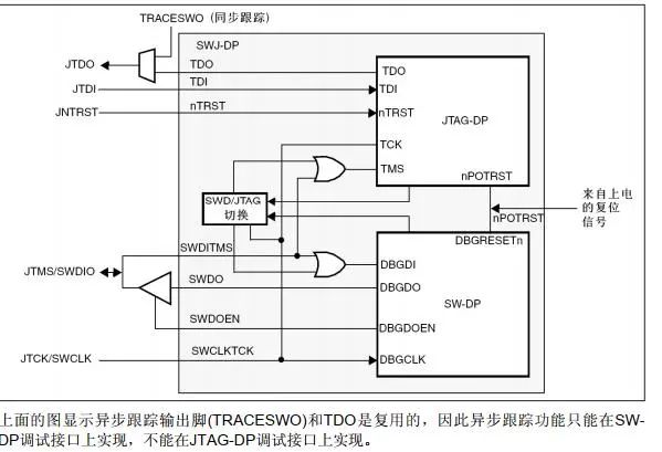
SWJ Debug Port
The mechanism for switching between JTAG-DP and SW-DP: The JTAG debugging interface is the default debugging interface. To switch to SW-DP, a specific JTAG sequence must be output on TMS/TCK (SWCLK SWDIO), which disables JTAG-DP and activates SW-DP. This method can only be activated through the two pins SWCLK and SWDIO.
The specified sequence is:
Output more than 50 cycles of SWCLK = 1 signal
Output 16 SWDIO signals 0111100111100111 (MSB)
Output more than 50 cycles of SWCLK = 1 signal
Note:If the SW-DP mode is used during debugging, the SWDIO and SWCLK signals can be observed, and the above signals should be observable without issues.
SWJ Debug Port Pins Note:All pins in the figure below exist in all STM32 series microcontrollers corresponding to the SWJ port.
After a system reset (SYSRESETn or PORRESETn), all five pins belonging to SWJ-DP are immediately initialized as dedicated pins callable by the debugger.However, the STM32 controller can remap and configure the debugging IO through the remapping and debugging IO configuration register (AFIO_MARR) to disable some or all pin functions of the SWJ-DP interface to be released as general IO ports. This register is mapped to the APB bridge of the Cortex-M3 system bus, and its configuration will be set by the user.
Note:In microcontroller development, it is almost never necessary to occupy the debugging interface.It is essential to ensure that the internal pull-up and pull-down on the JTAG pins are not floating, as they directly connect to D flip-flops controlling the debugging mode.Special attention must be paid to the SWCLK/TCK pins, as they directly connect to the clock terminals of some D flip-flops.
To avoid any uncontrolled I/O levels, the STM32F10xxx embeds internal pull-ups and pull-downs on the JTAG input pins.
● JINTRST:Internal pull-up
● JTDI:Internal pull-up
● JTMS/SWDIO: Internal pull-up
● TCK/SWCLK: Internal pull-down
Once the JTAG I/O is released by user code, the GPIO controller regains control.The states of these I/O ports will return to their reset state.
● JNTRST:Input with pull-up
● JTDI:Input with pull-up
● JTMS/SWDIO:Input with pull-up
● JICK/SWCLK:Input with pull-down
● JTDO:Floating input
Software can use these I/O ports as regular I/O ports.
Note:The JTAG IEEE standard recommends pull-ups on TDI, TMS, and nTRST, while there is no specific recommendation for TCK. However, in the STM32F10xxx, the JTCK pin has a pull-down.
The embedded pull-ups and pull-downs eliminate the need for external resistors, allowing the serial interface to be used while freeing unused debugging pins as general I/O ports. To utilize the serial debugging interface to release some general I/O ports, user software must set SWJ_CFG=010 after reset, thus releasing PA15, PB3, and PB4 for general I/O use.This is a point to remember, as I often forget this.


To help everyone learn better, Changxue Electronics has specially added a public account for microcontrollers and EDA, pushing relevant knowledge daily, hoping to assist your learning!