Digital Medium Transistor DACFET

 1. Introduction
Many electrical appliances used in daily life are equipped with power electronic conversion circuits. These circuits can convert AC input from a power line into DC, and then convert the obtained DC and the DC provided by batteries back into AC (necessary for the normal operation of motors). They can also perform voltage conversion for DC voltage step-up and step-down. Recently, initiatives to protect the Earth’s environment have led to the need for energy-saving measures in society, which has resulted in the selection of the most efficient power conversion circuits, namely SMPC (Switched Mode Power Conversion) circuits.
SMPC circuits consist of switching devices, diodes, and LCR components. By controlling the current/voltage with switching devices and utilizing the calculus functions of LC components, they can achieve the desired current/voltage output at the load end. The industry has been searching for switching devices that have high breakdown voltage in the off state (breakdown voltage: VBp), low on-resistance (Rn), and fast switching speeds (short switching times). Advances in power transistors based on Si semiconductor technology have improved the performance of SMPC circuits, enhancing conversion efficiency while achieving miniaturization and lightweight designs. Si semiconductor power transistors are primarily used in insulated gate field-effect transistors (MOSFETs for low voltage and IGBTs for high voltage) that achieve stable operation through simple driving circuits, allowing SMPC circuits to operate with over 90% efficiency.
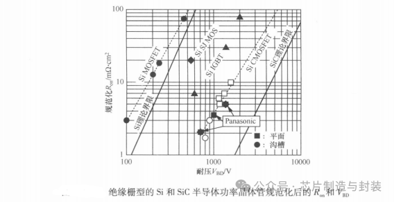
Switching devices using wide bandgap semiconductors like SiC can achieve higher VBD, lower Rsm, and shorter switching times, according to reports. The figure compares the normalized Ron and VBp of insulated gate Si and SiC power transistors. It can be seen from the figure that SiC devices exhibit high VBD and low Ro2 after surpassing the physical property limits of Si.

 2. SiC DACFET
SiC MOSFET is a unipolar device, and due to the superior physical properties of SiC, its channel resistance is more than an order of magnitude lower than that of Si MOSFETs. For example, under a VBp of 1000V, the Rg of Si IGBT (a bipolar device) can be reduced to less than half, while the switching time can be shortened to 100ns, especially exhibiting outstanding performance in high voltage applications above 1000V. By oxidizing the surface of SiC, a SiO2 insulating gate oxide film can be formed, but it cannot be asserted that the most perfect SiO2/SiC interface will always be formed. The formation of the SiO2/SiC interface determines the characteristics of SiC MOSFETs, such as Rc.
We propose a special structure that maintains a normally-off state by controlling the threshold voltage (Vth) and can reduce the MOS channel resistance that significantly affects Rom. By utilizing an epitaxially grown delta-doping layer as the MOS channel layer, we effectively improve the device characteristics, which we refer to as the vertical DACFET (Delta-doped Accumulation Channel FET).
The figure shows a schematic diagram of the DACFET structure mentioned above. The cell size of the prototype vertical DACFET device is 10.4×10.4μm2, surrounded by an array structure, with a protective ring at the outermost end. The active area is 0.157cm2, and the overall size of the prototype chip is 5.0×4.2mm2. The MOS channel part of this unique SiC DACFET is formed by stacking a thin epitaxial growth film on the surface of the p-well region formed by ion implantation.
During the epitaxial growth process, the doping concentration of nitrogen (N) in SiC changes dramatically, forming a delta-doping structure in the MOS channel layer with an i-layer that is almost undoped and an n-layer with a doping concentration above 10^18cm3. Afterward, oxidizing the surface of the outermost i-layer of the epitaxially grown MOS channel layer will form the SiO2/SiC interface, and the gate electrode will also be formed on this SiO2 oxide film.

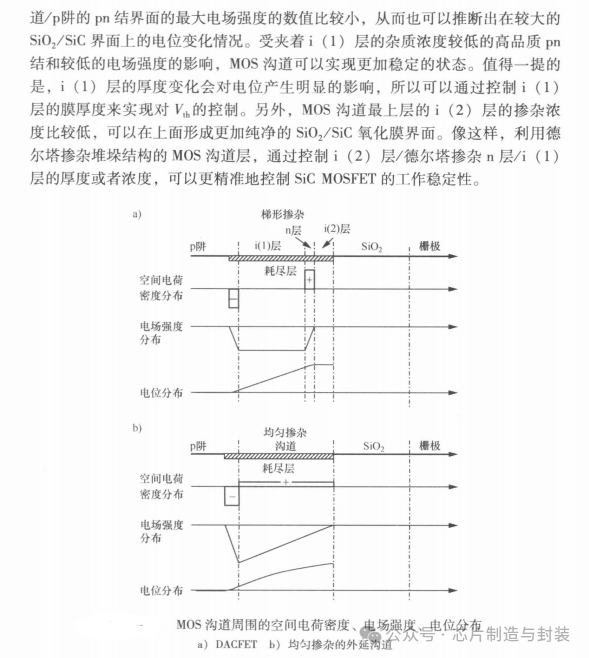
Next, we will use the simplest example of the MOS channel part of the SiC DACFET to illustrate the situation where a delta-doping layer is sandwiched in the i-layer. This simplest delta-doping stacked layer structure of the MOS channel is composed of (i(2) layer/delta-doping n-layer/i(1) layer). To observe the normally-off state of the MOS channel, a structure is designed to ensure that the MOS channel layer is essentially depleted without applying voltage to the gate electrode. Figure a shows the spatial charge distribution, electric field strength distribution, and potential distribution around the depleted layer of the MOS channel along the gate electrode/SiO2 oxide film/MOS channel/p-well.
The horizontal axis corresponds to the distance from the surface of the p-well upwards. Figure b shows the relevant data of the epitaxial channel under the same doping concentration for comparison. To ensure that the potentials at the SiO2/SiC oxide film interface in figures a and b are the same, normalization was performed. Additionally, the i-layer in the figure represents the ideal state of the i-layer, without considering the charges, electric field strength, or potential caused by traps at the oxide film interface or work function differences. As shown in figure a, the spatial charge of the depletion layer in the p-well and the spatial charge of the depleted delta-doping n-layer influence the i(1) layer sandwiched in between, presenting the same electric field distribution (trapezoidal). Comparing this electric field with the situation in figure b (triangular) under the same doping concentration, it can be observed that the former is in the MOS channel.

 3. Electrical Characteristics of SiC DACFET
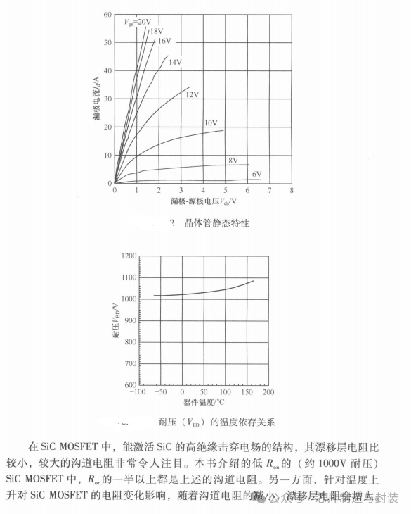
The figure shows the transistor characteristics of the prototype DACFET. The gate voltage Vg=0V to 20V, within this range, the controllable drain current Ia is above 40A (drain-source voltage Vds<1V). The characteristic on-resistance at Vg=20V is 3.5Ω·cm2. With this data, it can be determined that as a planar SiC MOSFET, it has good static characteristics. The device simulation is shown in the figure. The figure indicates the breakdown voltage situation above 1000V in the temperature range of -50~150℃. In the Vis above VBD, avalanche current flows, and limiting this current does not lead to device destruction.
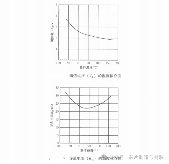
The Vth (I4 at gate voltage above 1mA) varies with temperature as shown in the figure. As the temperature rises, V1 decreases, and within the above temperature range, a normally-off characteristic above 1.8V can be observed, ensuring safe operation.

The overall R of the prototype SiC MOSFET cancels each other out, as shown in the figure, showing a minimum value change at room temperature (Ron(150℃)/Ron(room temperature) is about 1.3), compared to Si MOSFETs (for example, Roe(150℃)/Rgn(room temperature) is about 3), exhibiting a smaller temperature variation of Rn.
Especially when multiple devices are paralleled for high current switching, the presence of losses can cause the device temperature to rise. If the temperature coefficient of R02 is negative, it can lead to current concentration and the risk of breakdown. On the other hand, if the temperature coefficient is a relatively large positive value, the losses during operation will increase. SiC DACFET has a relatively small positive value, allowing for stable operation and maintaining low losses, making it an excellent characteristic as a power device.

In a switching experiment conducted at 300V/20A with the gate directly connected and maintaining a gate resistance of 0Ω, it was found that the switching time is below 10ns, which is very short. The switching time set for Si IGBT and other Si switching devices is generally above 100ns, so using SiC MOSFET in SMPC circuits can significantly reduce switching losses. In an actual 330V/2560W inverter circuit, it can be confirmed that switching losses can be effectively reduced by more than 60% compared to using Si IGBT.
As a vertical SiC MOSFET, SiC DACFET has a unique structure. This section has introduced information regarding its structure, characteristics, and operation. Experiments have also confirmed that using SiC power devices can achieve stable operation of SMPC circuits and reduce losses. In the future, further research is needed to clarify the advantages of SiC power devices, promote the rapid development of SiC electronic power technology, and contribute to energy conservation and environmental protection. Power electronics technology is bound to become widespread worldwide.

 For more inquiries, please followWeChat Official Account:Chip Manufacturing and Packaging
 Like
Like Share
Share Like
Like