GPIO stands for General Purpose Input/Output ports, which are pins that can be controlled by the STM32. GPIO pins connect to external hardware devices, enabling communication with external devices, controlling external hardware, or collecting data from external hardware.
Taking the STM32F103ZET6 chip as an example, this chip has a total of 144 pins, including 7 groups of general-purpose input/output ports (GPIO), namely GPIOA, GPIOB, GPIOC, GPIOD, GPIOE, GPIOF, GPIOG, with each GPIO group containing 16 GPIO pins. They are usually referred to as PAx, PBx, PCx, PDx, PEx, PFx, PGx, where x ranges from 0 to 15.
Most of the pins on the STM32 can also be reused as peripheral function pins (e.g., serial ports) aside from being used as GPIO.
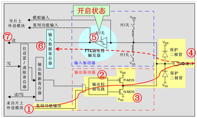
Basic Structure of GPIO
Each GPIO contains a circuit structure, which will be specifically introduced in the following sections of this article.
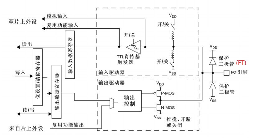
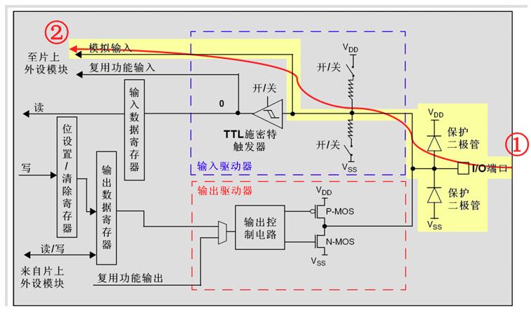
Explanation of Circuit Diagram
Protection Diodes: Two diodes on either side of the IO pin are used to prevent excessive voltage inputs from damaging the pins. When the pin voltage exceeds VDD, the upper diode conducts; when the pin voltage drops below VSS, the lower diode conducts, preventing abnormal voltage from entering the chip and causing damage. However, even so, high-power devices should not be directly connected; a power amplifier and isolation circuit must be added to prevent damage to the chip or ensure proper operation of external devices.
P-MOS and N-MOS Transistors: The unit circuit composed of P-MOS and N-MOS transistors allows GPIO to have “push-pull output” and “open-drain output” modes. The circuit will be analyzed in detail below.
TTL Schmitt Trigger: After passing through the trigger, the analog signal is converted into a digital signal of 0 and 1. However, when the GPIO pin is used as an ADC input channel to collect voltage, its “analog input” function is used, and at this point, the signal does not pass through the trigger for TTL level conversion. The ADC peripheral needs to collect the original analog signal.
It should be noted that when viewing the GPIO table in the “STM32 Chinese Reference Manual V10”, there is a column labeled “FT”, which indicates that this GPIO port is compatible with both 3.3V and 5V; if it is not marked “FT”, it means it is not compatible with 5V.
Operating Modes of STM32 GPIO
-
Floating Input (GPIO_Mode_IN_FLOATING)
-
Pull-Up Input (GPIO_Mode_IPU)
-
Pull-Down Input (GPIO_Mode_IPD)
-
Analog Input (GPIO_Mode_AIN)
-
Open-Drain Output (GPIO_Mode_Out_OD)
-
Open-Drain Multiplexed Output (GPIO_Mode_AF_OD)
-
Push-Pull Output (GPIO_Mode_Out_PP)
-
Push-Pull Multiplexed Output (GPIO_Mode_AF_PP)
Additionally, GPIO supports three maximum toggle speeds (2MHz, 10MHz, 50MHz). Each I/O port can be freely programmed, but the I/O port registers must be accessed as 32-bit words.
Floating Input Mode
Pull-Up Input Mode
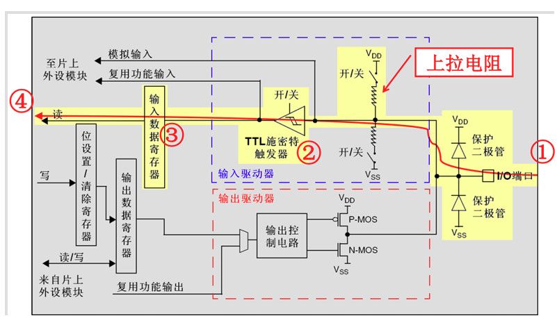
In pull-up input mode, the level signal of the I/O port directly enters the input data register. However, when the I/O port is floating (no signal input), the input level can be maintained at a high level; and when the input to the I/O port is low, the input level remains low.
Pull-Down Input Mode
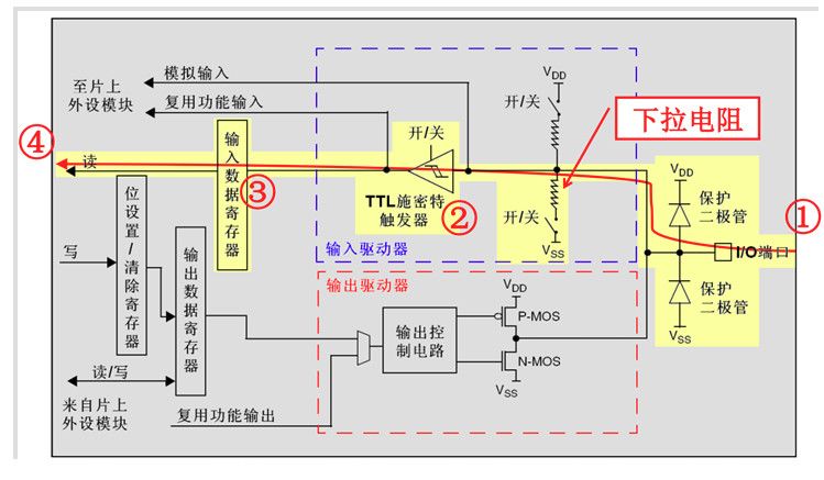
In pull-down input mode, the level signal of the I/O port directly enters the input data register. However, when the I/O port is floating (no signal input), the input level can be maintained at a low level; and when the input to the I/O port is high, the input level remains high.
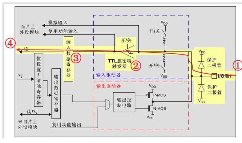
Analog Input Mode
In analog input mode, the analog signal (voltage signal, not level signal) of the I/O port is directly input into the on-chip peripheral module, such as the ADC module, etc.
Open-Drain Output Mode
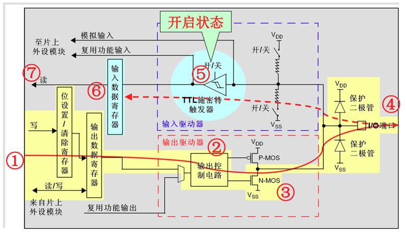
In open-drain output mode, by setting the bit in the set/clear register or the value of the output data register, through the N-MOS transistor, the output is finally sent to the I/O port. It should be noted that in this case, when the output value is set to high, the N-MOS transistor is off, and the level of the I/O port will not be determined by the output high or low, but by the pull-up or pull-down from the external circuit; when the output value is set to low, the N-MOS transistor is on, and the level of the I/O port will be low. At the same time, the level of the I/O port can also be read through the input circuit; note that the level of the I/O port is not necessarily the output level.
Open-Drain Multiplexed Output Mode
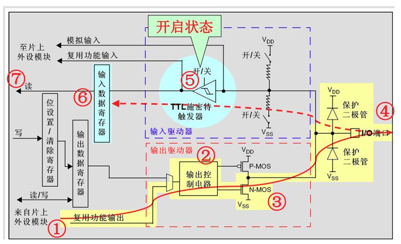
Open-drain multiplexed output mode is very similar to open-drain output mode. The only difference is that the source of the high and low levels is not directly written by the CPU to the output data register, but instead is determined by the output of the multiplexing function of the on-chip peripheral module.
Push-Pull Output Mode
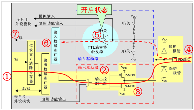
In push-pull output mode, by setting the bit in the set/clear register or the value of the output data register, through both P-MOS and N-MOS transistors, the output is finally sent to the I/O port. Here, note that when the output value is set to high, the P-MOS transistor is on and the N-MOS transistor is off, thus the level of the I/O port is determined by the P-MOS transistor: high level; when the output value is set to low, the P-MOS transistor is off and the N-MOS transistor is on, thus the level of the I/O port is determined by the N-MOS transistor: low level. At the same time, the level of the I/O port can also be read through the input circuit; note that at this time, the level of the I/O port must be the output level.
Push-Pull Multiplexed Output Mode
Push-pull multiplexed output mode is very similar to push-pull output mode. The only difference is that the source of the high and low levels is not directly written by the CPU to the output data register, but instead is determined by the output of the multiplexing function of the on-chip peripheral module.
1. What are Push-Pull Structures and Push-Pull Circuits?
2. What is the Difference Between Open-Drain Output and Push-Pull Output?
Open-Drain Output: Can only output a strong low level, while the high level relies on an external resistor to pull up. The output terminal is equivalent to the collector of a transistor. It is suitable for current-type drives, with a relatively strong current absorption capability (generally within 20mA);
Push-Pull Output: Can output strong high and low levels, suitable for connecting digital devices.
Regarding the push-pull output and open-drain output, the following simple diagram summarizes:
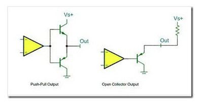
The left side of the diagram represents the push-pull output mode, where when the comparator outputs a high level, the lower PNP transistor is off while the upper NPN transistor is on, outputting a high level VS+; when the comparator outputs a low level, the situation is reversed, with the PNP transistor on, connecting the output to ground, resulting in a low level.
The right side can be understood as the open-drain output form, which requires a pull-up.
3. How to Choose I/O Modes in STM32?
Floating Input _IN_FLOATING – Floating input, can be used for KEY recognition, RX1.
With Pull-Up Input _IPU – IO with internal pull-up resistor.
With Pull-Down Input _IPD – IO with internal pull-down resistor.
Analog Input _AIN – Used for ADC analog input or low power consumption.
Open-Drain Output _OUT_OD – IO output 0 connects to GND, IO output 1 is floating, requiring an external pull-up resistor to achieve a high output. When the output is 1, the state of the IO port is pulled high by the pull-up resistor, but due to the open-drain output mode, the IO port can also be driven low or remain unchanged by external circuits. This allows for reading IO input level changes, achieving bidirectional functionality of C51 IO.
Push-Pull Output _OUT_PP – IO output 0 connects to GND, IO output 1 connects to VCC, reading the input value is unknown.
Multiplexed Push-Pull Output _AF_PP – On-chip peripheral functions (I2C’s SCL, SDA).
Multiplexed Open-Drain Output _AF_OD – On-chip peripheral functions (TX1, MOSI, MISO, SCK, SS).
Original text:https://blog.csdn.net/qq_38410730/article/details/79858906
Source from the internet, copyright belongs to the original author. If there is any infringement, please contact for deletion.