ESD: Electro-Static Discharge refers to the release of static electricity. Static electricity is a natural phenomenon that usually occurs through contact, friction, or induction between electrical devices. It is characterized by long-term accumulation, high voltage (which can reach thousands or even tens of thousands of volts), low charge, small current, and a short duration of action, often causing instability in electronic products or even damage.
EMI: Electromagnetic Interference refers to the disruption caused by electromagnetic waves. In high-speed PCB and system design, high-frequency signal lines, integrated circuit pins, and various connectors can become radiation interference sources with antenna characteristics, capable of emitting electromagnetic waves and affecting the normal operation of other systems or subsystems within the same system.
1) Isolation on the mold: Connectors should be as recessed as possible within the housing to increase the distance for static discharge to the internal circuit, weakening the energy, and changing the testing standard from contact discharge to air discharge, etc.;
2) Protect and isolate sensitive components during PCB layout. Sensitive modules such as RF, audio, and memory can be shielded with covers;
3) Place the RK3588 chip and core components in the center of the PCB. If they cannot be positioned in the center, ensure that the shield is at least 2mm away from the board edge and ensure that the shield is reliably grounded;
4) Layout the PCB according to functional modules and signal flow direction, ensuring that various sensitive parts are independent from each other. It is best to isolate parts that are prone to interference, such as DCDC switching power supply modules;
5) ESD components should be placed reasonably, generally at the source, that is, ESD components should be placed at the interface or static discharge point. The routing should go through the static discharge components first before being connected, as shown in Figure 1.

Figure 1 ESD Wiring Diagram
6) Component layout should be away from the board edge and maintain a certain distance from connectors. Generally, it is recommended to be at least 20mil from the board edge and more than 40mil from connectors;
7) The PCB surface must have a good GND return loop, and each connector should have a good GND connection loop on the surface. Those with shielding covers should be connected to the surface ground as much as possible, and more ground holes should be made at the soldering points of the shield. To achieve this, no routing should be done on the surface of each connector part, and there should be no large-scale cutting of the surface copper;
8) Do not route on the surface board edge and make more ground holes, and if necessary, properly isolate the signal from the ground, as shown in Figure 2;

Figure 2 Adding GND Holes at Board Edge
10) If there is a board-to-board connection via connectors, it is recommended to connect all signals in series with a certain resistance (between 2.2ohm-10ohm, depending on SI testing requirements), and reserve TVS devices to enhance anti-static surge capability;
11) The 100nF capacitor on the RK3588 nPOR pin must be placed close to the pin with an 8/16mil ground via. If space allows, it is recommended to place two or more for better grounding;
12) Key signals such as Reset, clock, and interrupt should be at least 5mm away from the board edge, and the routing below should have a reference plane to avoid edge effects, as shown in Figure 3.

Figure 3 Distance of Key Signals from Board Edge
9) Leave more exposed copper on the PCB to enhance the static discharge effect or facilitate the addition of foam and other remedial measures, as shown in Figure 4.
13) For other peripheral chips with Reset pins, it is recommended to add a 100nF capacitor close to the pin, and the capacitor’s ground pad must have an 8/16mil ground via. If space allows, it is recommended to place two or more for better grounding, as shown in Figure 5.

Figure 4 Exposed Copper Treatment on PCB

Figure 5 Placement of Capacitor Ground Holes
14) Isolate on the PCB to allow static electricity to only discharge in certain areas, such as connecting the ground pin of the socket through a separate hole to the inner ground layer, and keeping the surface PCB clear of ground copper as much as possible, allowing sensitive signals to be far from static discharge areas (surface ground copper), etc., as shown in Figure 6, isolating HDMI signals from ground.

Figure 6 Isolation of HDMI Signals from Ground
1) The three elements of electromagnetic interference: interference source, coupling channel, and sensitive devices, as shown in Figure 7. We cannot handle sensitive devices, so to deal with EMI, we can only start from the interference source and the coupling channel. The best way to solve EMI problems is to eliminate the interference source; if it cannot be eliminated, try to cut off the coupling channel or avoid the antenna effect;

Figure 7 Three Elements of EMC
2) It is generally difficult to completely eliminate interference sources on a PCB, but methods such as filtering, grounding, balancing, and impedance control can be used to improve signal quality (such as at the ends). Various methods are generally used in combination, but good grounding is the most basic requirement;
3) Common materials for dealing with EMI include shielding covers, dedicated filters, resistors, capacitors, inductors, ferrite beads, common mode inductors/ferrite cores, absorbing materials, and spread spectrum devices;
4) Filter selection principle: If the load (receiver) is high impedance (most single-ended signal interfaces are high impedance, such as SDIO, RBG, CIF, etc.), then choose capacitive filter devices to be included in the line; if the load (receiver) is low impedance (such as power output interfaces), then choose inductive filter devices to be included in the line. The use of filter devices should not cause the signal quality to exceed its SI permissible range. Differential interfaces generally use common mode inductors to suppress EMI;
5) Shielding measures on the PCB must be well grounded; otherwise, it may cause radiation leakage or the shielding measures may form an antenna effect. The shielding of connectors must comply with relevant technical standards;
6) RK3588 spread spectrum modules can be used. The degree of spread spectrum should be determined according to the signal requirements of the relevant parts. Specific measures can be found in the RK3588 spread spectrum documentation;
7) All clock series matching resistors are recommended to be retained to provide matching impedance and improve signal quality;
8) At the DC power input, if conditions permit, reserve a common mode inductor or EMI filter;
9) At interfaces such as USB, HDMI, VGA, and screen connectors, add reserved common mode inductors or filtering circuits;
10) When adding heat sinks, be aware that heat sinks can also couple EMI energy and produce radiation. When selecting heat sinks, in addition to meeting thermal design requirements, they should also meet EMI testing requirements. Heat sinks should reserve grounding conditions, and when grounding is needed, ground the heat sink. It is difficult to specify the number of grounding points and how to select grounding points, which needs to be adjusted based on actual conditions during laboratory testing of the first version of hardware;
12) The requirements for EMI and ESD layout are highly consistent. Most of the previously mentioned ESD layout requirements are applicable to EMI protection. Additionally, the following requirements should be added:
A. Ensure signal integrity as much as possible;
B. Differential lines should be of equal length and closely coupled to ensure the symmetry of differential signals, minimizing the misalignment of differential signals and avoiding conversion into common mode signals that cause EMI problems, as shown in Figure 8.

Figure 8 Symmetry of Differential Signals
C. For components with metal shells, avoid coupling interference signals to radiate. Also, avoid coupling the interference signals from the shell to other signal lines;
D. All clock series matching resistors should be close to the CPU end (source end), and the routing between the CPU pins and the resistors must be controlled within 400mil;
E. If the PCB exceeds 4 layers, it is recommended to let all clock signals run on the inner layers as much as possible;
F. Prevent power radiation; the copper covering of the power layer must be recessed, by a unit of H (the thickness of the medium between power and ground), with a recommended recess of 20H. We require the ground plane to be larger than the power or signal layers, which helps prevent external radiation interference and shield against external interference (generally, when designing the PCB, the power layer can be recessed 1mm from the ground layer; otherwise, strictly meeting 20H may make routing difficult, as shown in Figure 9).

Figure 9 20H Principle


5 Suggestions for DFM Manufacturability Analysis

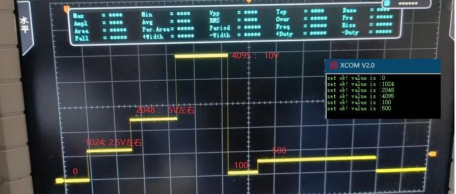
Implementation of 0~10V Output Circuit in Microcontroller

Scan to add customer service WeChat, note “Join Group” to pull you into the official technical WeChat group of Fan Yi Education, and exchange technical issues and insights with many electronic technology experts~