
Author | Wang WeifengSource | Automotive Electronics and Software
Whether it is the safety architecture design of the chip or the safety architecture design of related downstream systems, the safety aspect is primarily about addressing two types of failures during the product development process: random hardware failures and systematic failures.
Next, let’s discuss some considerations for the functional safety architecture design of chips at the hardware level.
Note: The chips mentioned below refer to processor-level III class hardware devices.
01. Reference for Hardware Safety Design Requirements of Chips
The hardware safety design of microcontrollers is typically achieved through “Safety Island”. Safety Island is a widely used concept, similar to the waiting area built for pedestrians at traffic lights at intersections. It can isolate pedestrian and vehicle traffic, preventing vehicles from losing control and hitting pedestrians. The safety island in a chip is also a specially designed independent area used to implement safety-related functions. Nowadays, many chips used in safety-critical fields often indicate that they have a safety island mechanism.
Generally, a subsystem or core on the chip that is specifically designed for a certain attribute (such as safety attributes) can be referred to as an “Island” concept, emphasizing the “independence” and “specificity” of local design. The collection of dedicated storage units, power supply modules, peripherals, communication buses, and other IPs used to support the chip’s proprietary functional safety can be collectively referred to as “Safety Island”. On the “island”, safety-related tasks can be executed relatively independently, and the safety island provides a physical environment for software to perform safety tasks.
Safety islands are usually independent of other systems and cores on the chip, requiring independent power domains, separate computing units, and internal modules and memory that must have physical isolation mechanisms, high-priority interrupt mechanisms, and even dedicated safety diagnostic units to diagnose problems occurring on the “island” in real-time and enter the corresponding safety state.
Next, starting from the minimal system, let’s discuss the implementation methods of the chip safety island.
The Dual-Core Lockstep (DCLS) architecture is a type of on-chip redundant integrated circuit architecture.ISO 26262 does not specifically propose requirements for on-chip redundant integrated circuit architectures, but IEC 61508-2 has proposed relevant requirements for integrated circuits with on-chip redundancy.
To use on-chip redundancy on the same semiconductor substrate,IEC 61508-2 has proposed a series of requirements. Using a single semiconductor substrate can achieve subsystems (on-chip redundancy) with hardware fault tolerance greater than zero. In this case, all of the following requirements must be met, and the design of the E/E/PE system and integrated circuits should comply with these requirements.
1 The highest safety integrity level that can be claimed for the integrated circuit functional safety described in this series of clauses is limited to SIL3.
2It cannot enhance system capability through the combination of components.
3To avoid common cause failures, the impact of temperature rise (for example, caused by random hardware failures) needs to be considered.
4Independent physical blocks should be established for each channel and each monitoring component (such as watchdog) of the integrated circuit substrate. These physical blocks should include bonding wires and pins. Each channel should also have independent inputs and outputs, without going through another channel.
5Appropriate measures should be taken to avoid hazardous failures caused by power supply failures, including common cause failures. Power supply failures include but are not limited to:
-
Noise.
-
Disturbances propagated through the power supply lines.
-
Asynchronous power supply switching, which may cause issues such as latch-up effects or high inrush currents.
-
Excessive current consumption caused by short circuits.
6The minimum distance between independent physical blocks should be sufficient to avoid short circuits and crosstalk between blocks.
7Short circuits and crosstalk between adjacent lines of independent physical blocks should not lead to functional safety failures.
8Regardless of the integrated circuit design process used, the substrate should be grounded.
9The sensitivity of integrated circuits with on-chip redundancy to common cause failures should be assessed by determining the B.3 definedβ factor, which is referred to asβIC In integrated circuits, the factorβIC should be used to replace theβ factor determined by the examples inGB/T 20438 Section 6 Appendix D and assess the safety integrity of the E/E/PE system.
10When a fault is detected in an integrated circuit with on-chip redundancy (through diagnostic tests, inspection tests, or other methods), specific actions should be taken to maintain a safe state.
11The minimum diagnostic coverage for each channel should be greater than 60%In the case where the monitoring component is executed only once, the minimum diagnostic coverage of that component should also be greater than 60%.
12If a watchdog is necessary (for example, to monitor program sequences and ensure necessary diagnostic coverage or safety failure scores), one channel should not be used as a watchdog for another channel unless using functionally diverse channels.
13When testing electromagnetic compatibility without additional safety margins, the functions performed by the integrated circuit should not be disturbed.
14When testing electromagnetic compatibility with additional safety margins, functional safety (including integrated circuits) should comply with the IEC 61326-3-1 defined FS criteria.
15For digital input ports connected to external asynchronous digital signals, appropriate measures should be taken to avoid hazardous failures caused by oscillation, such as using multi-level clock synchronization to introduce signals separately.
16Potential commonalities of shared resources, such as boundary scan circuits and special function register groups, should be analyzed.
17The common cause sources listed above from 1 ~ 15 are primarily used for integrated circuits with on-chip redundancy, and other relevant common cause sources specified by GB/T 20438 should also be considered.
Since the dual-core lockstep architecture belongs to the on-chip redundancy architecture, to reduce the impact of related failures, the following measures are generally required.( 1 Physical Diversity
-
The core hardware is spatially separated, at least 100µm apart, forming a physical “isolation zone”, referred to as “Safety Lake” in some chips.

Figure 1 Dual-Core Lockstep Physical Diversity Structure
-
One core is physically flipped and rotated 90° relative to the other. Figure 1 shows the physical diversity structure of the dual-core lockstep.
(2) Power Diversity
-
Each core has a dedicated power ring.
(3) Time Diversity
-
One core runs with a delay relative to the other core (for example, by 2 clock cycles), including an input delay and an output delay to ensure synchronization.
-
The CPU clock domain is divided into two clock trees, so that the clock is transmitted to the two CPUs through two independent paths.
02. Power Safety of Chips
The power supply module is a typical common cause failure source (DFI). In the chip design process, for safety reasons, it is necessary to provide independent power rails for the core logic circuits and I/O logic circuits (including analog-to-digital converters (ADC), flash pumps, and oscillators); while also equipping corresponding voltage monitoring modules to monitor functional anomalies of each power rail.
Safety chips typically have embedded voltage monitors that can detect out-of-range power supply voltage (OV/UV) conditions. When the power supply voltage is significantly above or below the rated value, the voltage monitor will drive the internal reset pin to ensure that the processor remains in a safe operating state. When the power supply voltage is within the normal range, the voltage monitor does not trigger a processor reset.
1. Reasons for Power Safety Design of Chips
The power supply module is a common infrastructure within the chip and has shared characteristics; generally, all functional modules in a chip require power to operate, while different modules require different operating voltages. How to avoid the impact of power crosstalk between different modules is one of the safety considerations in the chip design process. Typically, to eliminate or mitigate the impact of common cause failures, independent power supply modules are provided for redundant cores and I/O logic circuits.
Speaking of common cause failures, let’s first introduce the basic concept of this term.
-
Common Cause Failure (CCF): Failures that do not have statistical independence, meaning the probability of failure combinations does not equal the product of the probabilities of all considered independent failures.
In simple terms, common cause failure refers to the failure of two or more independent events that have a certain correlation, and the reasons for this correlation can be diverse. For example, if Xiao Wang and Lao Li work in the same office, and one day Xiao Wang starts coughing and has a runny nose, showing cold symptoms, and the next day Lao Li also shows cold symptoms, the events of both Xiao Wang and Lao Li showing cold symptoms have a certain correlation.
The correlation or mode of association that leads to failure varies; common cause failure includes common cause failures and cascading failures.
-
Common Cause Failure (CCF): Failures that occur simultaneously or within a short time due to a common cause affecting two or more components.
The cause of failure can be triggered by a single event or root cause (such as incidental causes, unassignable causes, noise, natural patterns, etc.), as shown in Figure 2.
Using the previous example of Xiao Wang and Lao Li, if Xiao Wang catches a cold and shortly after, Lao Li also shows cold symptoms, both Xiao Wang and Lao Li’s cold symptoms can be attributed to the flu virus, thus it is the flu virus that causes the “common cause failure” of Xiao Wang and Lao Li.
Common Mode Failure (CMF) is a subset of common cause failure. The coincidence of random failures in two or more (not necessarily identical) components in redundant channels leads to the same erroneous behavior in terms of functional safety.
Figure 3 illustrates two components within two different but redundant channels, where one root cause leads to two different failures (Failure 1, Failure 2), resulting in the same failure (Failure C) in both components and channels. Since the same failure occurs in both channels, the functional safety comparator mechanism cannot detect the failure.
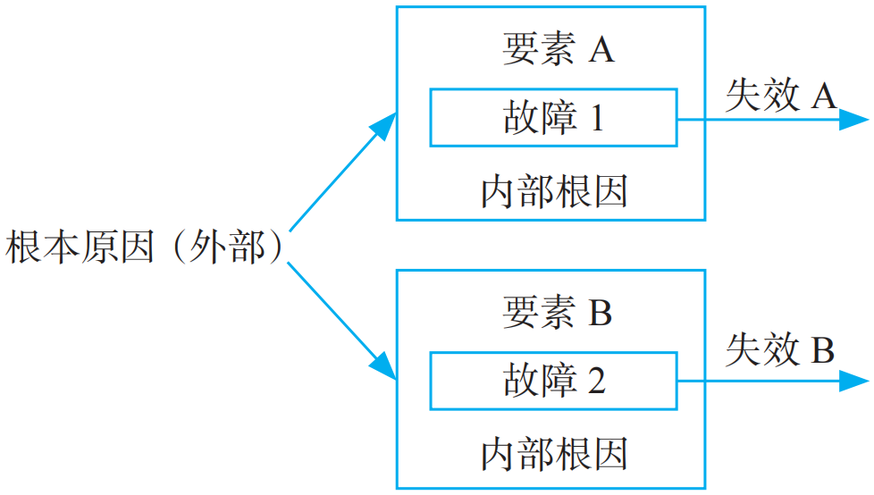
Figure 2 Common Cause Failure Diagram
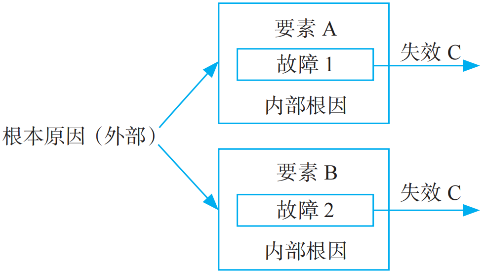
Figure 3 Common Mode Failure Diagram
Continuing with the previous example of Xiao Wang and Lao Li, both working in the same office, affected by the flu virus, they both exhibit symptoms of fever, cough, and nasal congestion, which prevents them from concentrating on work, leading them to interrupt their current tasks and take sick leave to go to the hospital. In this case, the flu virus caused a “common mode failure” for both Xiao Wang and Lao Li.
-
Cascading Failure (CF): When a local failure of a component in the system affects interconnected components, leading to the failure of another or multiple components within the same system and channel, a cascading failure occurs. Cascading failure is a related failure that is not a common cause failure. Figure 4 illustrates two components within a channel, where a single root cause leads to a failure in one component (Failure 1), resulting in a failure (Failure A). This failure then cascades to the second component, causing a second failure (Failure 2), which in turn leads to another failure (Failure B).
Figure 4 Cascading Failure Diagram
Cascading failure emphasizes the cascading of failures within the same system and channel. Continuing with the previous example of Xiao Wang and Lao Li, affected by the flu virus, Lao Li first experiences a sore throat leading to a cough, followed by severe nasal congestion causing loss of smell, and intermittent tinnitus leading to hearing loss. As Lao Li’s cough worsens, it leads to a respiratory infection causing throat swelling, damaging the vocal cords and preventing normal speech. In this case, the flu virus caused a “cascading failure” in Lao Li’s body affecting the ear, nose, and throat.
2. Examples of Power Safety Design for Chips
After introducing the relevant concepts of failure, we will now illustrate the measures typically taken in the chip design process to address potential failures caused by the power supply module.
Figure 5 shows a schematic diagram of internal components of a processor chip, with the bolded box indicating the voltage regulation component within the chip.
The voltage regulator (Embedded Voltage Regulator, EVR) in Figure 5 is identified as a shared resource within the chip, supplying power to other components through internal power networks. The schematic also shows a voltage monitoring module to monitor the voltage of the EVR.
EVR can supply power to each hardware element within the processor chip.
Assuming that during the development process according to functional safety standards, the following requirements are assigned to the processor chip.
-
MCU-REQ-2 :Random hardware faults leading to incorrect outputs from the central processing unit (CPU) should be detected within 20ms .
-
MCU-REQ-2.1 : The CPU should be monitored by a redundant CPU. The outputs of the CPU and redundant CPU should be compared by a hardware comparator at each clock cycle.
-
MCU-REQ-2.2 : When the outputs of the CPU and redundant CPU do not match, an error event should be generated.
Based on the above safety requirements for the internal components of the processor module, the implementation of MCU-REQ-2 involves FTA, resulting in the fault tree shown in Figure 6.
Based on the shared resources and redundancy elements identified in the above FTA, the relevant failure analysis regarding the power supply module in the processor is derived, as shown in Figure 7.
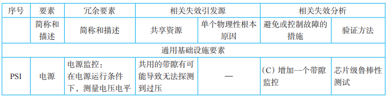
Figure 5 Schematic Diagram of Internal Components of a Processor Chip
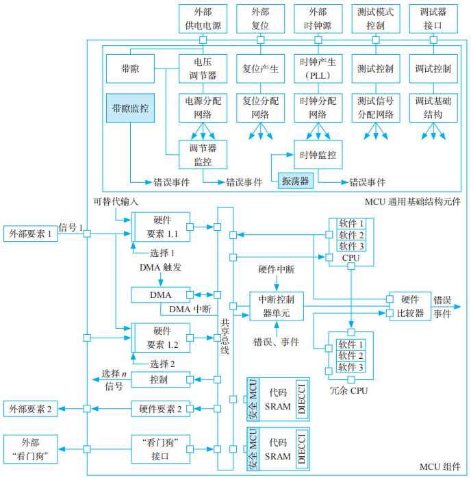 Figure 6 Example of Processor FTA 01
Figure 7 Example of Processor Power Supply Module DFA
Based on the above DFA results, new bandgap monitoring elements have been added to the original chip architecture to reduce the risk of failures related to bandgap drift failure modes. After considering the safety factors of the power supply module, relevant safety modules have been added to the architecture (see the light gray filled modules in Figure 8). The enhanced internal architecture of the processor chip is shown in Figure 8.
The above example is only to illustrate how safety attributes are considered in the chip design process. From the example, it can be seen that to achieve functional safety, the chip architecture design must undergo safety analysis to determine where to add circuits. From design to implementation and verification, a standard process must be followed to ensure safety integrity, consistency, and traceability.
Figure 8 Enhanced Internal Architecture of Processor Chip 01
03. Clock Safety of Chips
The clock management logic circuits within the chip typically include clock sources and clock generation logic circuits, where the clock generation logic circuits include clock multiplication of phase-locked loops (PLL), clock distributors, and clock distribution logic circuits.
For the component modules of the clock management logic circuit, taking a certain safety microcontroller as an example, the following detection circuits are typically considered in the chip design process to address various potential failure modes of the clock management logic circuit.
( 1 ) Low-Power Oscillator Clock Detector
The Low-Power Oscillator Clock Detector (LPOCLKDET) is a safety diagnostic tool used to detect failures in the main clock oscillator.LPOCLKDET uses an embedded high-frequency, low-power oscillator (HF LPO). The working principle of the clock detection circuit is to verify a certain clock (oscillator or HF LPO) between the rising edges of the remaining clocks. The results indicate that besides incorrect marking and frequency repetition, the circuit may also fail due to transient conditions.
(2 ) PLL Difference Detection
PLL logic circuits have embedded diagnostic functions to detect differences in PLL output clocks. This difference is caused by phase lock loss between the reference clock and the feedback clock. The error response and indication depend on the design of the PLL control registers within the system module.
(3) Dual Clock Comparators
One or more Dual Clock Comparators (DCC) are used for multi-purpose safety diagnostics. DCC can be used to detect incorrect frequencies and drift between clock sources. DCC consists of two counter blocks, one counter block serves as a reference clock, while the other serves as a test clock. Both the reference clock and test clock can be selected by software. The theoretical design ratio of the clock frequency between the reference clock and the test clock serves as the expected ratio of clock frequencies, and the deviation of the ratio of their actual test values from the expected ratio generates an error signal.
(4) External Clock Output Monitoring (ECLK)
Some processor chips provide the function of outputting selected internal clock signals for external monitoring. By editing the registers within the system module, software can configure this feature.
The processor clock circuit module is a typical common infrastructure module, and the related failures caused by random hardware failures also need to be considered in the chip design process, as shown in Figure 9. Continuing with the example of the internal components of the processor, the relevant failure sources (DFI) are identified through FTA, and then relevant failure analysis is conducted based on the identified DFI.
According to Figure 9, the clock identified as a related failure source, the relevant failure analysis regarding the clock circuit in the processor is derived, as shown in the circled content in Figure 10.
Based on the above DFA results, new oscillator elements have been added to the original chip architecture to reduce the risk of failures related to clock drift failure modes. After considering safety factors for the clock module, relevant safety modules have been added to the architecture (see the light gray filled modules in Figure 11). The enhanced internal architecture of the processor chip is shown in Figure 11.
Figure 9 Example of Processor FTA 02
Figure 10 Example of Processor Clock Module DFA 02
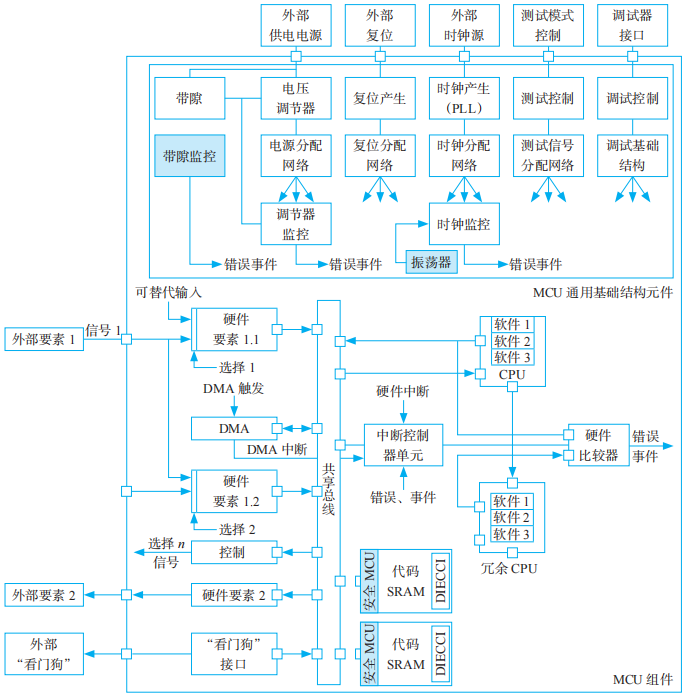 Figure 11 Enhanced Internal Architecture of Processor Chip 02
04. Storage Safety of Chips
During data addressing, writing, storing, and reading, the chip’s digital circuit components and memory are utilized. The following will discuss the storage safety of chips from these two aspects.
1. Failures
( 1 ) Digital Circuit Component Failures
The digital circuit components in the chip include microcontrollers, system-on-chip (SoC) devices, application-specific integrated circuits (ASIC), and field-programmable gate arrays (FPGA), etc.
Failures of digital circuit components in chips typically include the following types.
1 ) Permanent failures, also known as “hard errors” or “hard faults”, are described in detail as follows.
-
Stuck faults: The fault characteristic in the circuit is that regardless of how the input excitation changes, the node remains in a logical high (1) or logical low (0) state.
-
Open circuit faults: A fault that breaks a node into two or more nodes, thereby changing the number of nodes in the circuit.
-
Bridging faults: Refers to an accidental connection between two signals. Depending on the logic circuit used, it may produce logical functions of “OR” or “AND”. This fault typically occurs only between physically adjacent signals.
-
Single Event Hard Error (SHE): An irreversible change caused by a single radiation event, usually involving permanent damage to one or more elements in the device.
2) Transient faults (transient fault), also known as “soft errors” or “soft faults”, are described in detail as follows.
-
Single Event Transient (SET): A single high-energy particle passing through causes instantaneous voltage drift at a certain point in the integrated circuit (e.g., voltage spikes).
-
Single Event Upset (SEU): A soft error caused by a signal flip induced by a high-energy particle passing through.
-
Single Bit Upset (SBU): A flip of a single storage unit caused by a single particle.
-
Multiple Cell Upset (MCU): Multiple bits in the integrated circuit affected simultaneously by a single particle. The erroneous bits are usually (but not always) physically adjacent.
-
Multiple Bit Upset (MBU): Errors in two or more bits within the same half-byte, byte, or word caused by a single particle. Multiple bit upset cannot be corrected by simple error correction codes (ECC) (e.g., single bit error correction).
Single Event Transient (SET), Single Event Upset (SEU), Single Bit Upset (SBU), Multiple Cell Upset (MCU), and Multiple Bit Upset (MBU) are commonly referred to as “soft errors”. They are termed “soft errors” because the circuit itself is not permanently damaged by radiation.
(2) Memory Failures
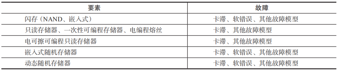
Memory failures may vary depending on the memory architecture and technology. Typical failures of semiconductor memory are shown in Table 1.
Table 1 Memory Failure Models
Soft errors occur when radiation events cause sufficient charge interference, leading to low-energy semiconductor storage units, registers, latches, or flip-flops to experience state reversals or flips.
Soft errors may be associated with various types of volatile memory, such as dynamic memory, static memory, register groups in microcontrollers, caches, pipelines, device (such as ADC, DMA, MMU) configuration registers, interrupt controllers, complex timers, etc. The sensitivity to α particles and neutrons is determined by core voltage and physical structure.
2. Failure Protection Measures
For failures of digital circuit components and memory, standards provide failure protection measures and achievable typical diagnostic coverage rates, as shown in Tables 6-9.
Modern safety microcontroller chips typically deploy relevant circuits to detect and correct bit errors in memory. Memory Protection Units (MPU) are security circuit modules specifically used in modern safety microcontroller chips to implement memory partitioning and isolation, preventing unauthorized access to different data storage areas.
05. Temperature Monitoring of Chips
Chips utilizing semiconductor technology perform optimally at suitable temperatures. Typically, high temperatures can lead to irreversible damage to chips, while functional anomalies caused by low temperatures are often recoverable. Abnormal temperatures (especially high temperatures) not only cause abnormal operation of the chip but also accelerate aging, affect the lifespan of the chip, and increase system power consumption, reducing the overall reliability of the system. Therefore, the impact of temperature is usually considered during the chip design process. For functional safety, temperature, as an environmental stress, is a typical failure source, so when implementing safety design chips, temperature sensors are typically deployed internally to monitor the chip’s internal temperature. Usually, each core in a microcontroller is equipped with a dedicated temperature sensor to monitor core temperature. When the temperature exceeds preset range values (e.g., -40℃~150℃), the temperature sensor outputs a temperature status signal, and the chip enters a Fail-safe state and outputs a fault signal to the upper system.
Deploying temperature sensors internally in the chip to monitor core temperature is a detection measure. In actual chip design processes, in addition to detection-type safety measures, we also consider preventive measures, such as the chip’s heat dissipation design. Similar to the comprehensive energy efficiency indicators of white goods, power consumption is also an important parameter for measuring chip performance. The internal heat dissipation design of the chip not only reduces power consumption and enhances performance but also helps meet the safety and integrity requirements of the chip. The following are some common chip heat dissipation technologies for reference.
-
Adding heat dissipation layers: Adding heat dissipation layers in the chip packaging to transfer the heat generated by the chip to the surface of the package, and then dissipate the heat through a heat sink. The heat dissipation layer can be made of conductive materials such as metal or ceramics.
-
Heat pipe technology: Heat pipes are efficient heat transfer elements that can transfer large amounts of heat in a small space. Inside the chip, heat pipes can be connected to the heat dissipation area of the chip to quickly transfer heat to the other end of the heat pipe, which is then dissipated through a heat sink.
-
Thermal design optimization: By optimizing the thermal design of the chip, reducing thermal resistance and centrally planning heat dissipation paths, heat dissipation efficiency can be improved. For example, rationally layout heating elements within the chip, optimize the chip’s heat dissipation channels, and improve the thermal conductivity of packaging materials.
Many other hardware safety measures are also deployed within the microcontroller architecture. For further understanding, it is recommended to study the chip safety manual and map it to the relevant standard requirements, which may be the most convenient way to achieve functional safety design for chips.