Introduction:
1、Function: Capable of performing addition, subtraction, multiplication, and division operations with up to four digits, retaining four decimal places for division; 4*4 matrix key input, LED LCD display for showing data; each key press triggers a buzzer response, and a marquee light is included, allowing the buzzer and LED light to be turned on and off via the keys.
2、Package Structure: Code and common simulation issues, Keil source code, Proteus simulation diagrams (versions 7.8 and 8.13), schematics, reference documents, function descriptions, simulation code execution, soldering notes, free PPT templates, component lists, structural block diagrams, flowcharts, physical images, production processes, and must-read before use.
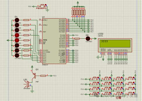
3、Simulation Structure: AT89C51, LCD display, 4*4 matrix keys, 8 indicators, buzzer
4、Code Files: Approximately 620 lines of code with comments, around 9000 words of documentation.
5. Obtain: Click the link at the bottom to read the original text or copy the link below into your browser to obtain the Keil source code and Project Backups simulation diagrams:
https://mall.bilibili.com/neul-next/detailuniversal/detail.html?isMerchant=1&page=detailuniversal_detail&saleType=10&itemsId=12083744&loadingShow=1&noTitleBar=1&msource=merchant_share
C+26
Some reference designs are as follows:
Abstract
In recent years, the development of microcontroller technology has been rapid, with electronic products being updated at an astonishing pace. Calculators are one of the most common electronic products in daily life. How can we make calculator technology more mature, fully utilize existing software and hardware conditions, and design a more outstanding calculator?
This design is a calculator simulation system based on the AT89C51 microcontroller, using a 4×4 matrix keyboard for input, capable of performing addition, subtraction, multiplication, and division operations with signed four-digit numbers, and displaying the operation process on an LCD1602.
The advancement of technology has eliminated the need for complex analog circuits; a microcontroller of just a few square centimeters can replace many cumbersome circuits. Currently, scientific calculators are widely used, which differ significantly from the simple calculators we use daily. In addition to performing basic arithmetic operations, scientific calculators can also handle positive number operations, powers, and roots, and have functions for exponentiation, logarithms, trigonometric functions, inverse trigonometric functions, and storage. The future of calculators is miniaturization and portability; solar-powered calculators and calculators designed with ACIC, such as those implemented purely in software, are emerging on the market. The future of intelligent calculators will be our development direction, and we hope to become widely used calculation tools.
Chapter 1 Introduction
1.1 Background of System Development
With the development of society and the advancement of science, people’s living standards are gradually improving, especially with the rapid development of microelectronics technology, which has changed dramatically. The fast update speed of electronic products is no longer surprising. Calculators are one of the most common electronic products in daily life. How to make calculator technology more mature, fully utilize existing software and hardware conditions, and design a better calculator to better serve various industries has become an important research topic in the electronic field today.
1.2 Significance of System Development
Today, calculators have become indispensable in people’s daily lives, appearing in various corners of society, such as stores, offices, and schools. Therefore, designing a simple and practical calculator has significant practical implications.
1.3 Design Objectives
This design aims to further master theoretical knowledge of microcontrollers, understand the hardware and software design of embedded microcontroller systems, and strengthen the ability to design practical application systems. Through this design study, I will master the basic methods of microcontroller program design and microcomputer interface applications, and be able to comprehensively apply the software and hardware knowledge learned during my undergraduate studies to analyze practical problems, improving my ability to solve practical problems in graduation design, laying a solid foundation for microcontroller applications and development.
1. To have a clear understanding of the working principles of character LCD display modules, such as initialization, clearing the screen, displaying, calling, and external characteristics, and to be able to use the LCD (liquid crystal display module) to display calculation results; master the driving and programming of the LCD display module, design the interface circuit between the LCD and the microcontroller, and utilize the microcontroller to drive and operate the liquid crystal module;
2. By fully analyzing the concept of internal logic, conducting software and debugging, learn to use and be able to design hardware circuits and software programs for a simple calculator with arithmetic capabilities based on this platform.
Chapter 2 Scheme Demonstration
2.1 Scheme Concept
Two design schemes can be adopted: one using FPGA as the core processing chip, equipped with corresponding peripherals; the other using the AT89C51 processor, equipped with corresponding peripherals.
1. Scheme One: Using FPGA Control
FPGA is a high-density programmable logic device. Since Xilinx launched the first FPGA in 1985, the integration density and performance of FPGAs have improved rapidly, with integration densities reaching over 5 million gates per chip and system performance up to 200MHz. Due to the high integration of FPGA devices, ease of use, and short development and market cycles, they have been rapidly popularized and applied in digital design and electronic production, dominating the field of high-density programmable logic devices.
However, for FPGA based on CRAM programming, the programming information must be stored in external memory, requiring external memory chips, and the usage method is complex with poor confidentiality. For a simple calculator, using FPGA is somewhat overkill and too costly.
2. Scheme Two: Using AT89C51
A microcontroller is a single-chip microcomputer, also known as a microcontroller (MCU). It typically consists of a single integrated circuit chip that contains the basic functional components of a computer: a central processing unit (CPU), memory, and I/O interface circuits. Therefore, as long as the microcontroller is combined with appropriate software and external devices, it can become a microcontroller control system. Microcontrollers are widely used in smart products, smart instruments, measurement and control technology, and smart interfaces, with advantages such as simple operation, practical convenience, and low cost. Among them, the AT89C51, with MCC-51 as its core, is the most typical representative of microcontrollers, applied in various control fields.
2.2 Scheme Comparison and Selection
Through the demonstration and comparison of the above two schemes, based on the practicality, convenience, and cost of the design, the AT89C51 microcontroller was chosen as the central processing unit for the calculator design, enabling the implementation of four-digit addition, subtraction, multiplication, and division operations with four decimal places.
Chapter 3 System Hardware Design and Description
3.1 System Composition and Overall Block Diagram
Figure 3.1 System Composition and Overall Block Diagram
3.2 Component Introduction
3.2.1 Features of AT89C51
Figure 3.2.1-1 Microcontroller AT89C51
1. Main Performance:
(1) • 8031 CPU compatible with MCC-51
• 8K bytes of programmable FLASH memory (lifetime: 1000 write/erase cycles)
• Fully static operation: 0Hz-33MHz
• Three-level encrypted program memory
• 128*8 bits internal RAM
• 32 programmable I/O lines
• Three 16-bit timers/counters
• Eight interrupt sources
• Full-duplex UART serial channel
• Low-power idle and power-down modes
• Interrupt wake-up after power-down
• Watchdog timer
• Dual data pointers
• Power-down identifier
• On-chip oscillator and clock circuit
(2) Pin Description:
VCC: Power supply voltage.
GND: Ground.
2. Functional Characteristics of AT89C51
AT89C51 is a low-power, high-performance CMOS 8-bit microcontroller with 8K in-system programmable FLASH memory. It is manufactured using Atmel’s high-density non-volatile memory technology and is fully compatible with the instruction set and pin configuration of industrial 80C51 products. The on-chip FLASH allows program memory to be programmed in-system, suitable for conventional programmers. With a clever 8-bit CPU and in-system programmable FLASH, the AT89C51 provides a highly flexible and efficient solution for numerous embedded control applications.
AT89C51 has the following standard features: 8k bytes of FLASH, 256 bytes of RAM, 32 I/O port lines, a watchdog timer, 2 data pointers, three 16-bit timers/counters, a 6-vector 2-level interrupt structure, a full-duplex serial port, and on-chip crystal oscillator and clock circuit.
Additionally, the AT89C51 can operate down to 0Hz in static logic, supporting two software-selectable power-saving modes. In idle mode, the CPU stops working, allowing RAM, timers/counters, serial ports, and interrupts to continue functioning. In power-down mode, the RAM content is preserved, the oscillator is frozen, and all microcontroller operations stop until the next interrupt or hardware reset. The 8-bit microcontroller has 8K bytes of in-system programmable FLASH. The chip is available in three package forms: PDIP, TQFP, and PLCC, to meet different product needs.
9C51 Pin Functionality
The AT89C51 microcontroller is a 40-pin chip as shown in Figure 3.2.1-2.
Figure 3.2.1-2 AT89C51 Pin Diagram
(1) Ports: P0, P1, P2, P3 are four 8-bit ports.
P0 Port: P0 is an 8-bit open-drain bidirectional I/O port. As an output port, each bit can drive 8 TTL logic levels.
Writing a “1” to the P0 port makes the pin act as a high-impedance input.
When accessing external program and data memory, the P0 port is also used as the low 8 bits of the address/data multiplexed. In this mode, P0 does not have internal pull-up resistors.
During FLASH programming, the P0 port is also used to receive instruction bytes; during program verification, it outputs instruction bytes. During program verification, external pull-up resistors are required.
P1 Port: P1 is an 8-bit bidirectional I/O port with internal pull-up resistors, and the P1 output buffer can drive 4 TTL logic levels. Writing a “1” to the P1 port pulls the port high via the internal pull-up resistor, allowing it to be used as an input port. When used as an input, the pin pulled low externally will output current (IIL) due to internal resistance.
Additionally, P1.0 and P1.1 serve as external count input (P1.0/T2) and trigger input (P1.1/T2EX) for Timer/Counter 2, respectively, as shown in the table below.
During FLASH programming and verification, the P1 port receives the low 8 bits of the address byte.
Pin Number Second Function:
P1.0 T2 (External count input for Timer/Counter T2), clock output
P1.1 T2EX (Trigger signal and direction control for Timer/Counter T2)
P1.5 MOCI (for in-system programming)
P1.6 MICO (for in-system programming)
P1.7 CCK (for in-system programming)
P2 Port: P2 is an 8-bit bidirectional I/O port with internal pull-up resistors, and the P2 output buffer can drive 4 TTL logic levels. Writing a “1” to the P2 port pulls the port high via the internal pull-up resistor, allowing it to be used as an input port. When used as an input, the pin pulled low externally will output current (IIL) due to internal resistance.
When accessing external program memory or reading external data memory with a 16-bit address (e.g., executing MOVX @DPTR), the P2 port outputs the high eight bits of the address. In this application, the P2 port uses strong internal pull-ups to send a “1”.
When using an 8-bit address (e.g., MOVX @RI) to access external data memory, the P2 port outputs the contents of the P2 latch.
During FLASH programming and verification, the P2 port also receives the high 8 bits of the address byte and some control signals.
P3 Port: P3 is an 8-bit bidirectional I/O port with internal pull-up resistors, and the P3 output buffer can drive 4 TTL logic levels. Writing a “1” to the P3 port pulls the port high via the internal pull-up resistor, allowing it to be used as an input port. When used as an input, the pin pulled low externally will output current (IIL) due to internal resistance.
The P3 port is also used for special functions of the AT89C51 (second functions) as shown in Table 3.2.1.
Table 3.2.1 P3 Port Pin Alternate Functions:
Port Pin Second Function
P3.0 RXD (Serial input)
P3.1 TXD (Serial output)
P3.2 /INT0 (External interrupt 0)
P3.3 /INT1 (External interrupt 1)
P3.4 T0 (External input for Timer 0)
P3.5 T1 (External input for Timer 1)
P3.6 /WR (External data memory write enable)
P3.7 /RD (External data memory read enable)
During FLASH programming and verification, the P3 port also receives some control signals.
Additionally, the P3 port receives some control signals used for FLASH memory programming and program verification.
(2) Other Pin Descriptions:
RCT: Reset input. When the crystal oscillator is working, a high level on the RCT pin for 2 machine cycles will reset the microcontroller. After the watchdog timer completes, the RCT pin outputs a high level for 96 crystal oscillator cycles. The DICRTO bit on the special register AUXR (address 8EH) can disable this function. By default, the reset high level is effective.
ALE/PROG – When accessing external program memory or data memory, the ALE (Address Latch Enable) outputs pulses to latch the low 8 bits of the address. Generally, ALE outputs a fixed pulse signal at 1/6 of the clock oscillation frequency, so it can output a clock externally or be used for timing purposes. Note that an ALE pulse will be skipped each time external data memory is accessed.
During FLASH memory programming, this pin is also used to input programming pulses (PROG).
If necessary, the ALE operation can be disabled by setting the D0 bit in the special function register (CFR) area at address 8EH. After this bit is set, only a MOVX and MOVC instruction can activate ALE. Additionally, this pin is weakly pulled high, and when the microcontroller executes external programs, the ALE disable bit should be set to invalid.
PCEN – Program Storage Enable (PCEN) output is the read enable signal for external program memory. When the AT89C51 fetches instructions (or data) from external program memory, the PCEN is valid twice per machine cycle, outputting two pulses. During this time, when accessing external data memory, the PCEN signal will be skipped twice.
EA/VPP – External Access Enable. To make the CPU access only external program memory (address 0000H-FFFFH), the EA pin must remain low (grounded). Note that if the encryption bit LB1 is programmed, the EA pin state will be latched during reset.
If the EA pin is high (connected to Vcc), the CPU will execute instructions from the internal program memory.
During FLASH memory programming, this pin receives +12V programming enable power Vpp, which must be used with a 12V programming voltage Vpp.
Ground Ground
a. Internal Mode b. External Mode
Figure 3.2.1-3 External Crystal Oscillator Structure Pin Diagram
XTAL1 is the input of the on-chip oscillator’s inverting amplifier, while XTAL2 is the output. When using an external oscillator, the external oscillation signal should be directly applied to XTAL1, while XTAL2 is left floating. In internal mode, the clock generator divides the oscillation pulse frequency by two; for a crystal frequency of 12MHz, the clock frequency will be 6MHz. The frequency of the crystal can be selected between 1MHz and 24MHz; in this design circuit, a frequency of 12MHz is chosen. The capacitor is approximately 20PF. The machine cycle = 12 × time period; for a 12MHz machine cycle, it is 1 microsecond.
(3) Control or Reset Pins
RECET: This pin can reset the microcontroller when it is high (for about 2 machine cycles).
RCT/VPD – When a high level appears for two machine cycles, the microcontroller resets. After reset, P0 to P3 output high levels; the CP register is set to 07H; all other registers are cleared to 0; RAM status is unaffected. As shown in Figure 3.2.1-4.
Figure 3.2.1-4 Key Level Reset
The AT89CXX series microcontrollers implement ICP download functionality, replacing the download method of the 89CXX series. As a result, ATMEL has stopped producing the 89CXX series microcontrollers, and the AT89CXX available on the market is mostly stock from before discontinuation.
4. Programming Method for AT89C51
Before programming, the address, data, and control signals must be set according to the programming mode table; the sequence is as follows:
① Apply the address signal of the unit to be programmed on the address line.
② Apply the data byte to be written on the data line.
③ Activate the corresponding control signals.
④ Apply +12V programming voltage to the EA/Vpp pin.
⑤ For each byte written to the FLASH memory array or each programming secret bit written, add an ALE/PROG programming pulse. The writing cycle for each byte is self-timed, mostly around 50uC. Change the address of the programming unit and the data to be written, and repeat steps ①-⑤ until all files are programmed.
The current status and development direction of microcontrollers:
Microcontrollers were born to meet the needs of industrial control and are the core components of automatic control systems. Therefore, they are mainly used in industrial control, intelligent instruments, household appliances, etc. They have advantages such as small size, multiple functions, low cost, ease of use, and flexible system design, and their application fields are constantly expanding. In addition to industrial control, intelligent instruments, communication, and household appliances, microcontroller chips are also widely used as core control components in high-end intelligent electronic toy products.
Since microcontrollers are primarily aimed at industrial control, they often operate in harsh environments, including high temperatures, strong electromagnetic interference, and even corrosive gases. Microcontroller control systems operating in space must also have radiation resistance, which determines that microcontroller CPUs have different technical characteristics and development directions compared to general-purpose microcomputer CPUs:
(1) High reliability;
(2) Strong control functions, often with complex numerical calculations;
(3) The instruction system is much slower than general-purpose microprocessors;
(4) Replacement of X series chips;
(5) Strong anti-interference capability and wide operating temperature range.
3.2.2 LCD1602 Liquid Crystal Display
1. Application Overview
The module has an internal character generator memory (CGROM), which includes Arabic numerals, uppercase and lowercase English letters, commonly used symbols, and Japanese kana. Each character has a fixed code; for example, the code for the uppercase letter “A” is (41H). When displaying, the module sends the code 41H to the LCD module, allowing us to see the letter “A” on the LCD.
The LCD1602 module has a total of 11 control instructions, and the rich instructions can complete LCD timing control, working mode settings, and data display.
The adopted LCD1602 module is a standard 16-pin socket, and the interface circuit is shown in Figure 3.2.3. Detailed information about the LCD1602 can be found in Table 3.2.3-1 and Table 3.2.3-2.
Figure 3.2.3 LCD Interface Circuit
Table 3.2.3-1 LCD1602 Pin Description
Pin 1 VCC is the ground power supply
Pin 2 VDD connects to the 5V positive power supply
Pin 3 V0 is the contrast adjustment terminal for the LCD display; when connected to the positive power supply, the contrast is weakest, and when connected to ground, the contrast is highest. If the contrast is too high, it will produce “ghosting”; a 10K potentiometer can be used to adjust the contrast.
In practical circuits, a 2K resistor to ground is used, which is quite ideal.
Pin 4 RC is the register select; high level selects the data register, low level selects the instruction register.
Pin 5 RW is the read/write signal line; high level performs read operations, low level performs write operations.
When both RC and RW are low (00), instructions or display addresses can be written; when RC is low and RW is high (01), busy signals can be read; when RC is high and RW is low (10), data can be written.
Pin 6 E is the enable pin; when E transitions from high to low, the LCD module executes the command.
Pins 7-14 D0-D7 are 8-bit bidirectional data lines.
Pins 15-16 are the backlight anode and cathode.
Table 3.2.3-2 LCD1602 Instruction Table
Instruction 1 Clear Display Instruction Code 01H, cursor resets to address 00H;
Instruction 2 Cursor Reset Instruction Code 02H, cursor returns to address 00H;
Instruction 3 Cursor and Display Mode Settings
I/D bit → Cursor moving direction, high level moves right, low level moves left;
C bit → Whether all text on the screen moves left or right, high level is effective, low level is ineffective;
Instruction 4 Display Switch Control
D bit → Controls the overall display on and off, high level indicates display on, low level indicates display off;
C bit → Controls whether the cursor is on or off, high level indicates cursor on, low level indicates cursor off;
B bit → Controls whether the cursor blinks, high level blinks, low level does not blink;
Instruction 5 Cursor or Display Shift
C/C bit → High level moves displayed text, low level moves cursor;
Instruction 6 Function Command Settings
DL bit – high level indicates a 4-bit data bus, low level indicates an 8-bit bus;
N – low level indicates single-line display, high level indicates double-line display;
F – low level indicates 5×7 dot matrix characters, high level indicates 5×10 dot matrix characters;
Instruction 7 Character Generator RAM Address Setting
Instruction 8 DDRAM Address Setting
Instruction 9 Read Busy Signal and Cursor Address
BF bit → Busy flag bit, high level indicates busy, at this time the module cannot receive commands or data;
Instruction 10 Write Data
Instruction 11 Read Data
2. Characteristics of LCD:
(1) Low voltage micro-power;
(2) Flat structure;
(3) Passive display type (no glare, does not irritate the eyes, does not cause eye fatigue);
(4) Large information display capacity (because pixels can be made very small);
(5) Easy to colorize (can reproduce very accurately on the color spectrum);
(6) No electromagnetic radiation (safe for the human body, beneficial for information confidentiality);
(7) Long lifespan (this device has almost no degradation issues, thus has a very long lifespan, although the backlight has a limited lifespan, it can be replaced).
Chapter 4 Design Principle Analysis
4.1 Determination of Design Scheme
This design requires the use of an LCD display and an encoding keyboard. Therefore, static display and an encoding keyboard are chosen. The LCD display will show the calculation results.
The main program initializes, while other programs are selected in a modular manner. Each module is debugged first, and once a module is successfully debugged, it is added to the main program one by one, ultimately completing the entire software design.
4.2 Calculator Hardware Scheme and Hardware Resource Allocation
4.2.1 Hardware Resource Allocation
Main hardware used: AT89C51 LCD display encoding keyboard
Hardware allocation:
1. P1 and P3 ports: Used as output ports to control the LCD display to show the results.
2. P2 port: Used as an input port connected to the keyboard for data input.
3. LCD display outputs the display.
4.2.2 System Hardware Design
To better achieve the system’s functionality, the design of the hardware circuit should follow these principles:
1. Optimize the hardware circuit
Using a combination of software design and hardware design; although using software to implement the functions of the hardware system may result in longer response times than using hardware alone, and it also occupies the time of the microcontroller (MCU), implementing hardware functions through software can simplify the hardware structure and improve circuit reliability. Therefore, in designing this system, while ensuring reliability and real-time performance, it is preferable to implement hardware functions through software as much as possible.
2. Reliability and Anti-Interference Design
According to reliability design theory, the fewer chips used in the system, the longer the average fault-free time of the system. Moreover, the fewer chips used, the less likely the address and data buses are to be interfered with on the circuit board. Therefore, the design philosophy of the system is to strive to use fewer chips while meeting functionality.
3. Flexible Function Expansion
Whether function expansion is flexible is an important indicator of a system’s quality. A single design often cannot fully consider all aspects of the system, and the system needs to be continuously improved and upgraded. When expanding functions, it should be based on the original design, modifying software programs and a small amount of hardware. For this system, it requires that the system hardware remains unchanged while being able to upgrade and expand functions through software program modifications.
Based on the proposed system design scheme and the above three principles, the hardware design of the system was determined. The calculator mainly consists of the following functional modules: non-encoding keyboard module, LCD display module, etc.
The hardware design of the system adopts a modular design approach. The AT89C51 microcontroller and the LCD display circuit are the core of the entire circuit, fulfilling the system’s functional requirements.
The simple calculator mainly includes: keyboard circuit, display circuit.
The following diagram shows the overall hardware structure. (As shown in Figure 4.2.2, this is the schematic of the entire system)
Figure 4.2.2 Calculator Schematic
The previous description outlines the design of the system, which adopts a relatively simple design scheme, so the total peripheral circuit of the system will not produce excessive interference. In the following description, the peripheral circuits of the system will be introduced separately. The keyboard part uses an encoding keyboard, and the display part uses an LCD display, which can fully meet the display requirements.
4.2.3 Keyboard Circuit Design
Keyboards can be divided into two categories: encoding keyboards and non-encoding keyboards. Encoding keyboards are a combination of many keys (more than 20) and dedicated driver chips. When a key is pressed, it can handle key bounce, multiple presses, etc., directly outputting the key code without requiring system software intervention. The standard keyboard used in general computers is an encoding keyboard. In smart instruments, parallel interface chip 8279 or serial interface chip HD7279 can be used to form an encoding keyboard, while also accommodating the display driving of digital tubes, and the related interface circuits and interface software can be found in the chip documentation. When the system’s functionality is complex and the number of keys is large, using an encoding keyboard can simplify software design. Non-encoding keyboards are low-cost.
From a cost perspective, this design uses a non-encoding keyboard. As shown in Figure 4.2.3
Figure 4.2.3 Encoding Keyboard Circuit
4.2.4 Display Circuit Design
When the system needs to display a small amount of data, using an LCD display is an economical and practical method. The P0 port serves as the data port for the LCD display, while the P3.5-P3.7 ports serve as its control ports, controlling the LCD display to output data.
The final circuit is shown in Figure 4.2.4:
Figure 4.2.4 LCD Display Output
Chapter 5 Software Design of the Calculator
5.1 Software Planning for the Calculator
The program for the simple calculator mainly includes the following functional modules:
1. Timing key scanning module, divided into read key program, key judgment program segment, operation subroutine, etc.;
2. Display module based on the LCD display;
3. Main module for system initialization.
5.2 Keyboard Scanning Program Design
The keyboard scanning subroutine first reads the low four bits of P1, then reads the high four bits of the P1 port. The key values are then cached. The key values are converted to ASCII codes, allowing software to set the content represented by each hardware key.
The read key program uses the inversion method to read keys, regardless of the size of the keyboard matrix, performing two key reads. The first time, all row lines output low levels to read all keyboard information (column information); the second time, all column lines output low levels to read all row lines (row information).
When a number key is pressed, the corresponding number is sent to the cache, and when a function key is pressed, the corresponding program is executed.
5.3 Display Module Program Design
The display module program first initializes the display module; then controls the cursor position; defines the control ports for the LCD display using the CBIT instruction; then sets clear screen, turn off display, return to position, turn on display, and the starting address of the display position, etc.
The flowchart of the display module is shown in Figure 5.3:
5.4 Main Program Design
The main program is primarily used to initialize the LCD display.
5.5 Software Reliability Design
Measures to improve the reliability of this instrument include:
1. To prevent program runaway, software traps are set.
2. To prevent program deadlock, watchdog technology is used in the software.
Conclusion
During the hardware production process, I encountered many detours, mainly because I started making it before I was very confident in the system design. Later, I found that there were deviations from the design requirements, and I had to revise it several times, wasting a lot of time and effort. I realized that designers need to be patient and carefully study the requirements from the beginning. The software writing process was also very labor-intensive because the requirements for software writing are high and require great attention to detail; a small mistake can lead to incorrect calls. I deeply realized that as a software programmer, one must never be careless. The speed and quality of completing a program are closely related to attention to detail. During programming, I fully utilized structured thinking. This approach resulted in fewer statements, making debugging easier, and allowing each functional module to be debugged one by one, fully demonstrating the advantages of structured programming. When each module was completed, integrating their functions completed the overall design.
Acknowledgments
I would like to express my heartfelt gratitude to my mentor, Professor XXX, for his enthusiastic guidance during this graduation project. Professor XXX is approachable and cares about students’ design progress and learning. In the early stages of the graduation project, he introduced us to many useful materials and books; he provided meticulous guidance in hardware design; during the debugging process, he offered timely advice on every issue that arose. During the writing phase of the graduation thesis, he asked us to submit drafts for review in advance, pointing out issues with content, font, and formatting one by one. His calm demeanor, serious work ethic, and rigorous academic attitude left a deep impression on me. More importantly, he is good at communicating with students, providing timely guidance not only in graduation design but also offering valuable advice for my final stage of university study. All of this has subtly influenced me and set a good example for my future career.
I would also like to thank Professor XXX, who cares about students’ progress, understands the troubles we face during the writing process, and provides us with a lot of help.
Finally, I sincerely thank everyone who has helped and cared for me!