 Follow our WeChat subscription account: Mechanical Industry Press E-World
Long press the QR code above to recognize and follow us!
Click the “Skill Improvement” menu to learn professional knowledge and download free resources!
Reply “Lottery” to enter the lottery activity page to participate!
The printed circuit board is abbreviated as PCB. It consists of an insulating substrate, connecting wires, and pads for assembling and soldering electronic components, serving both as conductive pathways and an insulating base.
1
Design of Printed Circuit Boards

The design of printed circuit boards is based on the designer’s intent, following the electrical schematic of the electronic product and the dimensions of the components, to arrange the electronic components reasonably and achieve electrical connections, transforming the electrical schematic into a printed circuit board layout and determining the processing technical requirements. The circuit design of printed circuit boards must consider the complexity of the circuit, the shape and weight of the components, the size of the working current, and the voltage of the circuit, in order to select suitable substrate materials and determine the type of printed circuit board. When designing the routing of printed wires, the working frequency of the circuit must also be considered to minimize the parasitic capacitance and inductance between wires.
The conditions that the design of printed circuit boards must meet are as follows.
1) According to the overall design requirements of the machine, the circuit diagram has been determined, and all components of the circuit have been selected, with their models and specifications confirmed.
2) Special requirements for certain components have been determined, such as which components need shielding, which need frequent adjustments or replacements; which wires need to use shielded cables; and the environmental conditions in which the circuit operates, such as temperature, humidity, and atmospheric pressure have been clarified.
3) The connection form between the printed circuit board and other parts of the machine (or submachine) has been determined, and the models and specifications of the sockets and connectors have been confirmed.
1.Main Content of PCB Design
PCB design includes circuit design and packaging design (i.e., printed wire design) in two parts.
The main contents of PCB design include:
(1) Familiarizing oneself with and mastering the dimensions, packaging forms, lead types, pin arrangements, functions of each pin, and their shapes in the schematic, thereby determining the installation positions and other requirements such as heat dissipation and reinforcement for the components.
(2) Identifying electromagnetic interference sources in the circuit and sensitive components susceptible to external interference, and determining measures to eliminate interference.
(3) Arranging wires and components based on electrical and mechanical performance, determining the installation methods, positions, and dimensions of components, and determining the width of printed wires, spacing, pad diameter, and hole spacing, etc.
(4) Determining the size, shape, materials, types of printed circuit boards, and external connections and installation methods.
For circuits primarily composed of discrete components that are not too complex, a single-sided board design can be adopted; for more complex circuits with many integrated circuits, a double-sided board design can be used.
2.Steps and Methods of PCB Design
When starting the design of printed circuit boards, designers should follow relevant rules and standards, referring to relevant technical documents. For example, Figure 1 shows the design steps. The technical documents specify a series of sizes, layers, component sizes, coordinate grid spacing, spacing for soldered components, and the process for creating printed circuit board graphics.
 Figure 1 Design Steps for Printed Circuit Boards
In the design steps, the selection of materials for printed circuit boards must consider electrical and mechanical properties, of course, price and manufacturing costs must also be considered, so as to select the substrate for printed circuit boards. Electrical properties refer to the insulation resistance, arc resistance, resistance of printed wires, breakdown strength, shear strength, and hardness of the substrate. The thickness of the printed circuit board should be determined from a structural perspective, mainly considering the weight-bearing capacity of the circuit board for all components mounted on it and the mechanical load capacity it will bear during use. If only small power components such as integrated circuits, small power transistors, resistors, and capacitors are mounted on the printed circuit board, and there are no strong load vibration conditions, a thickness of 1.5mm (for dimensions within 500mm × 500mm) is sufficient. If the board is larger or the support strength is insufficient, a thickness of 2 to 2.5mm should be chosen. The thickness of printed circuit boards has been standardized, with common sizes of 1.0mm, 1.5mm, 2.0mm, and 2.5mm, with 1.5mm and 2.0mm being the most commonly used.
For very small printed circuit boards such as calculators and electronic watches, thinner copper foil laminated boards can be used to reduce weight and lower costs.
(1) Selection of materials, thickness, and board dimensions for printed circuit boards, determining external connections, and determining installation methods for components.
The size of the printed circuit board is closely related to its processing and assembly, and should be considered from the perspective of assembly technology in two aspects: on one hand, it should facilitate automated assembly, making full use of the equipment’s performance and allowing the use of generalized, standardized tools and fixtures; on the other hand, it should facilitate the assembly of printed circuit boards into products of different specifications, ensuring easy installation and reliable fixation.
1) Material selection. Material selection must consider electrical and mechanical properties, relative purchasing prices, and relative manufacturing costs.
2) Determining thickness. Thickness selection primarily considers the weight-bearing capacity of all components mounted on the printed board and the mechanical load capacity it will bear during use.
3) Shape and dimensions. The structural dimensions of the printed board should consider two aspects from the perspective of assembly technology: on one hand, it should facilitate automated assembly, making full use of the equipment’s performance and allowing the use of generalized, standardized tools and fixtures; on the other hand, it should facilitate the assembly of printed circuit boards into products of different specifications, ensuring easy installation and reliable fixation.
The shape of the printed circuit board should be as simple as possible, generally rectangular, and irregular boards should be avoided. The dimensions of the printed circuit board should be as close to standard sizes as possible to simplify processes and reduce processing costs.
The thickness of multilayer printed circuit boards should also be determined based on the electrical performance and structural requirements of the circuit.
(2) The design of the arrangement of components on the printed circuit board is used to determine the width, spacing, and diameter of pads and hole sizes for the printed wires.
When manually drawing PCB diagrams, it is possible to use graph paper to accurately express the coordinate positions of components on the printed circuit board. In designing and drawing coordinate dimension diagrams, it should be based on the circuit diagram and consider the layout and routing requirements, including which components are on the board, which need reinforcement, heat dissipation, and shielding; which components are outside the board, how many external connections are needed, and how the lead positions are determined. If necessary, a wiring diagram for external components should also be drawn.
A typical component is a representative component in geometric dimensions among all components that need to be installed. It serves as the basic unit for arranging components. Then, estimate the sizes of other large components in multiples of the typical component (i.e., how many typical components a large component is equivalent to in geometric dimensions), so that the overall size needed for the printed circuit board can be calculated.
Resistor and capacitor components, transistors, etc., should use standard pitches as much as possible to facilitate the automatic forming of component leads. The center of each component’s mounting hole must be positioned at the intersection of the coordinate grid.
The arrangement of components on the printed circuit board mainly includes three types: irregular arrangement (as shown in Figure 2), coordinate arrangement (as shown in Figure 3), and coordinate grid arrangement (as shown in Figure 4). Typical component arrangement is shown in Figure 5.
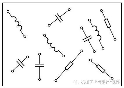 Figure 2 Irregular Arrangement
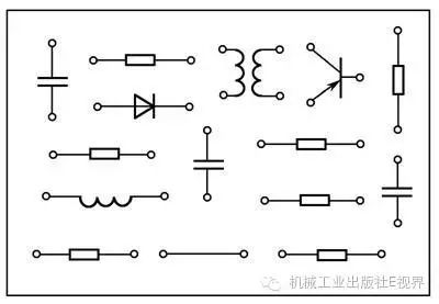 Figure 3 Coordinate Arrangement
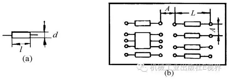 Figure 4 Coordinate Grid Arrangement
 (a) Typical Component (Assembly) Size (b) Typical Component Arrangement
Figure 5 Typical Component Arrangement PCB Diagram
(3) Design of Ground Lines on Printed Circuit Boards
1) Generally, the common ground line is arranged on the edge of the printed circuit board, leaving a certain distance for convenient installation and mechanical processing, which is beneficial for improving the circuit’s insulation properties.
2) In designing high-frequency circuits, to reduce lead inductance and ground impedance, and to prevent self-excitation, the ground line should have sufficient width.
3) The ground line of each level of the circuit on the printed circuit board can generally be designed as a self-closing loop. However, in the presence of strong magnetic fields from the outside, closed loops formed by ground lines should be avoided to prevent electromagnetic induction from affecting the electrical performance of the circuit.
(4) Design of Input and Output Terminals
1) Input and output terminals should be arranged in order of signal flow, making signal circulation easier and reducing parasitic interference between wires;
2) Input and output terminals should be as far apart as possible, and where possible, it is best to isolate them with ground lines. This can reduce mutual interference between input and output signals.
(5) Design of Wiring Diagrams
A wiring diagram refers to a diagram that uses simple lines to represent the direction of printed wires and the connection relationships of components. As shown in Figure 6.
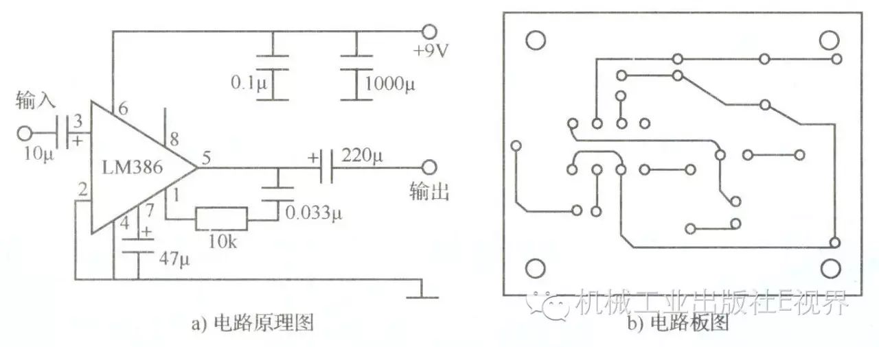 Figure 6 Wiring Direction from Schematic to Printed Board
(6) Sketching the Printed Circuit Board Diagram Based on the Electrical Schematic
First, the wiring direction and the positions of major components must be determined.
Once the wiring direction is determined, the first step is to determine the layout of unit circuits and their main components, such as transistors, integrated circuits, etc. Then, layout special components, and finally determine the method and position for external connections.
The drawing of the schematic generally relies on the signal flow and the role of components in the diagram, hence there are many crossing lines in the schematic, which does not affect reading the diagram. However, crossing lines in the printed circuit board are not allowed, so in the layout, a single line without crossings should be drawn first, which can be resolved by rearranging the positions and orientations of components. In more complex circuits, it may be difficult to avoid all crossings; in such cases, “flying leads” can be used to resolve issues. “Flying leads” refer to cutting a wire at the intersection on the printed circuit board and connecting it with a short wire from the component side. Excessive use of flying leads will affect the efficiency of component installation and cannot be considered a successful design, so they should only be used as a last resort.
3.Layout of Printed Circuit Boards
(1) Overall Layout
Before laying out the printed circuit board, a deep understanding of the circuit schematic is essential. Only with a thorough understanding of the circuit principles can a correct and reasonable layout be achieved. During the layout, care should be taken to avoid mutual interference between different levels of circuits and components. Such interferences include electric field interference—capacitive coupling interference, magnetic field interference—inductive coupling interference, high-frequency and low-frequency interference, high voltage and low voltage interference, as well as thermal interference. The layout should also meet design specifications and comply with production processing and assembly requirements, considering the convenience of circuit debugging and maintenance. A thorough understanding of the electrical characteristics and physical properties of the components used in the circuit is critical, including the rated power, voltage, current, working frequency, and physical characteristics such as size, width, height, and shape. The overall layout of the printed circuit board should also consider the stability of the center of gravity of the entire board, appropriate density of components, and aesthetic arrangement.
Components on printed circuit boards are generally divided into regular arrangement and irregular arrangement.
Regular arrangement, also known as neat arrangement, arranges components according to certain rules or directions. This arrangement, due to the restrictions of component positions and orientations, results in longer and more complex wiring distances, increasing interference between circuits. It is generally used only when the circuit operates at low voltage and low frequency (below 1MHz). The advantage of regular arrangement is its neatness and beauty, and it facilitates mechanized drilling and assembly.
Irregular arrangement, also known as close arrangement, does not have restrictions on component positions and orientations, and arranges components based on electrical connections, resulting in shorter and simpler wiring distances and less interference between circuits, which is beneficial for reducing distributed parameters, suitable for layouts of high-frequency (above 30MHz) circuits. The disadvantage of irregular arrangement is its untidy appearance and difficulty in mechanized drilling and assembly.
(2) Component Layout
For single-sided printed circuit boards, components can only be installed on the side without printed circuits, and the leads of components are soldered onto the pads of printed wires through mounting holes. For double-sided printed circuit boards, components should also be installed as much as possible on one side to facilitate processing, installation, and maintenance.
Components on the board should be arranged in a straight line as much as possible according to the order of the electrical schematic, aiming for compact and dense circuit installations to shorten leads and reduce distributed capacitance, which is particularly important for high-frequency circuits.
If it is necessary to divide the entire circuit into several blocks for installation due to special circuit requirements, each assembled printed circuit board should function independently to facilitate individual debugging and maintenance.
To rationally arrange components, minimize volume, and improve mechanical strength, an “auxiliary board” can be installed outside the main printed circuit board to mount bulky components such as transformers, inductors, large capacitors, and relays, which is beneficial for processing and assembly.
When placing components, the mutual influence between them should be considered. The orientation of components should cross with adjacent printed wires, and inductive components should be placed to prevent electromagnetic interference, with the axis of coils perpendicular to the board surface to minimize electromagnetic interference between installed components.
Heat-generating components in the circuit should be placed in positions conducive to heat dissipation, and if necessary, can be placed separately or equipped with heat sinks to facilitate cooling of the components themselves and reduce impact on adjacent components. Large and heavy components should be placed as close as possible to the fixed end of the printed circuit board to lower their center of gravity, increasing the mechanical strength and resistance to vibration and shock of the entire board, while reducing the load and deformation of the printed circuit board.
(3) Layout of Printed Wires
1) Layout of Ground Wires
① Generally, the common ground wire is arranged on the edge of the printed circuit board to facilitate installation on the frame and connection with the frame (ground). Wires should leave a certain distance (not less than the board thickness) from the edge of the printed circuit board, which not only facilitates the installation of rails and mechanical processing but also improves the circuit’s insulation properties.
② Inside each level of the circuit, care should be taken to prevent ground impedance interference caused by local currents, and it is best to adopt a single-point grounding principle. However, in actual wiring, absolute adherence to this principle may not be possible, and the goal should be to arrange them within a common area as much as possible.
③ When the circuit operates at frequencies above 30MHz or in high-speed switching digital circuits, to reduce ground impedance, large-area covering ground wires are often used. In this case, grounding of internal components at each level should also adhere to the single-point grounding principle, meaning grounding within a small area.
2) Layout of Input and Output Wires
To minimize parasitic coupling between wires, the layout should follow the order of signal flow, and the input and output terminals should be kept as far apart as possible, ideally isolated by ground lines. If the input and output terminals are too close, and the output wire is too long, parasitic coupling will occur.
3) Layout of High-Frequency Circuit Wires
For high-frequency circuits, it is essential to keep the leads of high-frequency wires, transistor electrodes, input, and output lines short and straight. If the distance between wires is small, they should avoid running parallel to each other. High-frequency circuits should avoid external wires crossing; if many crossing wires are needed, it is best to use double-sided printed circuit boards, with crossing wires printed on both sides of the board. In double-sided boards, printed wires on both sides should avoid running parallel to each other to minimize parasitic coupling, preferably arranged vertically or at an angle.
4) External Connections of Printed Circuit Boards
Printed circuit boards can be connected externally in various ways, depending on the structural requirements of the entire machine. Generally, the following two methods are adopted.
① Interconnection with wires: The points that need to be connected externally should first be brought to one end of the printed circuit board using printed wires, and the wires should enter the solder holes from the back of the soldering points.
For circuits with special needs, such as connecting high-frequency high-voltage external wires, they should be brought out at suitable positions and should not run along with other wires to avoid mutual interference.
② Interconnection with plug-in connectors: The printed circuit board’s end is shaped like a plug for insertion into a socket with contact springs. Using pinhole plugs and sockets, fixing holes are set on both sides of the pinhole plug to secure it to the printed circuit board, with a 90° bent pin connecting to the printed circuit board contact and the other end inserted into the socket.
5) Connection Pads
Connection pads, also known as solder pads, refer to the metallic parts around the solder holes of printed wires for external lead soldering. The size of the connection pads depends on the size of the solder holes. Solder holes are the holes that allow the leads of components or jumper wires to pass through the substrate. Clearly, the diameter of the solder holes should be slightly larger than the diameter of the leads of soldered components. The size of solder holes is related to the process; when the solder hole diameter is greater than or equal to the thickness of the printed circuit board, punching can be used; when the solder hole diameter is less than the thickness of the printed circuit board, drilling can be used. Generally, the specifications for solder holes should not be excessive.
The diameter of the connection pad D should be greater than the inner diameter of the solder hole d, generally taken as D=(2~3)d, to ensure soldering and bonding strength.
The shapes of connection pads vary, with round pads being the most commonly used, as they naturally form a smooth conical shape when soldering, resulting in strong and aesthetically pleasing bonds. However, sometimes square, oval, and elongated pads are also used to increase adhesion strength.
6) Printed Wires
If the connection between pads is integrated, it resembles an island on water, hence called an island pad. Island pads are often used in irregular arrangements of components, facilitating component density and fixation while significantly reducing the length and number of printed wires. Moreover, when pads and printed wires are integrated, the area of copper foil increases, greatly enhancing the peel strength of the pads and printed wires. Island pads are commonly used in high-frequency circuits as they can reduce the inductance of connections and increase the shielding area of ground wires, minimizing parasitic coupling between connections.
When designing printed circuit boards, once the layout of components and wiring is preliminarily determined, the specific design of printed wires and the graphics of the printed circuit board must be carried out. At this point, issues such as the width of printed wires, spacing between wires, and other design dimensions and graphics formats will inevitably arise. The size and graphic format of wires cannot be chosen arbitrarily, as they relate to the overall dimensions and electrical performance of the printed circuit board.
7) Drawing of Positioning Holes and Positioning Methods
① Width of Printed Wires
In general, printed wires should be as wide as possible, which is beneficial for carrying current and facilitates manufacturing. The relationship between the width of a 0.05mm thick copper foil wire and the allowable current and its own resistance can be calculated.
When determining the width of printed wires, in addition to considering current-carrying capacity, attention should also be paid to its peel strength on the board and coordination with connection pads, generally taking wire width b=(1/3~2/3)D. The typical wire width can range from 0.3 to 2.0mm, with recommendations for 0.5mm, 1.0mm, 1.5mm, and 2.0mm specifications, where 0.5mm wire width is mainly used for miniaturized electronic products.
Printed wires themselves also have resistance, which generates heat and causes voltage drop when current flows through. The resistance of printed wires can generally be ignored, but when acting as a common ground wire, the resistance value should be considered to avoid potential differences caused by ground wires leading to parasitic feedback.
Electrical and grounding wires in printed circuits carry larger currents, so they should be appropriately widened during design, generally taken as 1.5~2.0mm.
When low resistance and inductance of printed wires are required, wider signal wires can be used; when low distributed capacitance is required, narrower signal wires can be used.
② Spacing of Printed Wires: Generally, the spacing between wires should equal the wire width but should not be less than 1mm; otherwise, it will be difficult to use the immersion soldering method when soldering components. For miniaturized devices, the minimum spacing should not be less than 0.4mm. The choice of wire spacing is related to the soldering process; when using immersion soldering or wave soldering, the spacing should be larger, while when using manual soldering, the spacing can be slightly smaller.
In high-voltage circuits, high potential gradients exist between adjacent wires, and their influence must be considered. Breakdown between printed wires can lead to carbonization, corrosion, and cracking of the substrate surface. In high-frequency circuits, wire spacing will affect the size of distributed capacitance, thus impacting circuit loss and stability. Therefore, the choice of wire spacing should be comprehensively determined based on substrate materials, working environments, and the size of distributed capacitance. The minimum wire spacing is also related to the processing methods of printed circuit boards, which should be considered when selecting.
③ Shape of Printed Wires: The shapes of printed wires can be divided into straight uniform shapes, diagonal uniform shapes, curved uniform shapes, and curved non-uniform shapes. As shown in Figure 7.
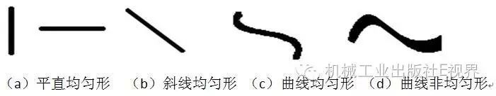 Figure 7 Shape of Printed Wires
The graphics of printed wires must consider mechanical factors, electrical factors, and also the aesthetic appearance of the wire graphics. Therefore, when designing the graphics of printed wires, the following principles should be followed as shown in Figure 8.
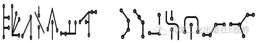 Figure 8 Shapes of Printed Wires
When designing the graphics of printed wires, the following principles should be adhered to:
① The width of wires (except for ground wires) on the same printed circuit board should preferably be the same;
② Printed wires should be straight and should not have sharp bends or angles; all bends and transitions must be connected with arcs;
③ Printed wires should avoid branches as much as possible; if branches are necessary, they should be smooth;
④ Printed wires should avoid long-distance parallels; printed lines on double-sided layouts should not run parallel but should cross each other;
⑤ If large areas of copper foil are needed on the printed circuit board, such as in the grounding sections of the circuit, the entire area should be hollowed out in a grid pattern to allow for rapid heating during immersion soldering and ensure uniform tin coating. Grid copper foil can also prevent deformation of the printed circuit board due to heat, and prevent copper foil from warping and delaminating.
4.Computer-Aided Design of Printed Circuit Boards
(1) PCB CAD
The design of printed circuit boards directly affects the quality and electrical performance of the product. With the development of the electronics industry, the demand for various types of printed circuit boards has increased, requiring shorter design and manufacturing cycles. Traditional manual design no longer meets production needs, and modern computer developments provide powerful means for CAD design of circuit schematics and printed circuit board graphics. The PCB CAD file is essentially a file containing the design information of the printed circuit board, structured as shown in Figure 9.
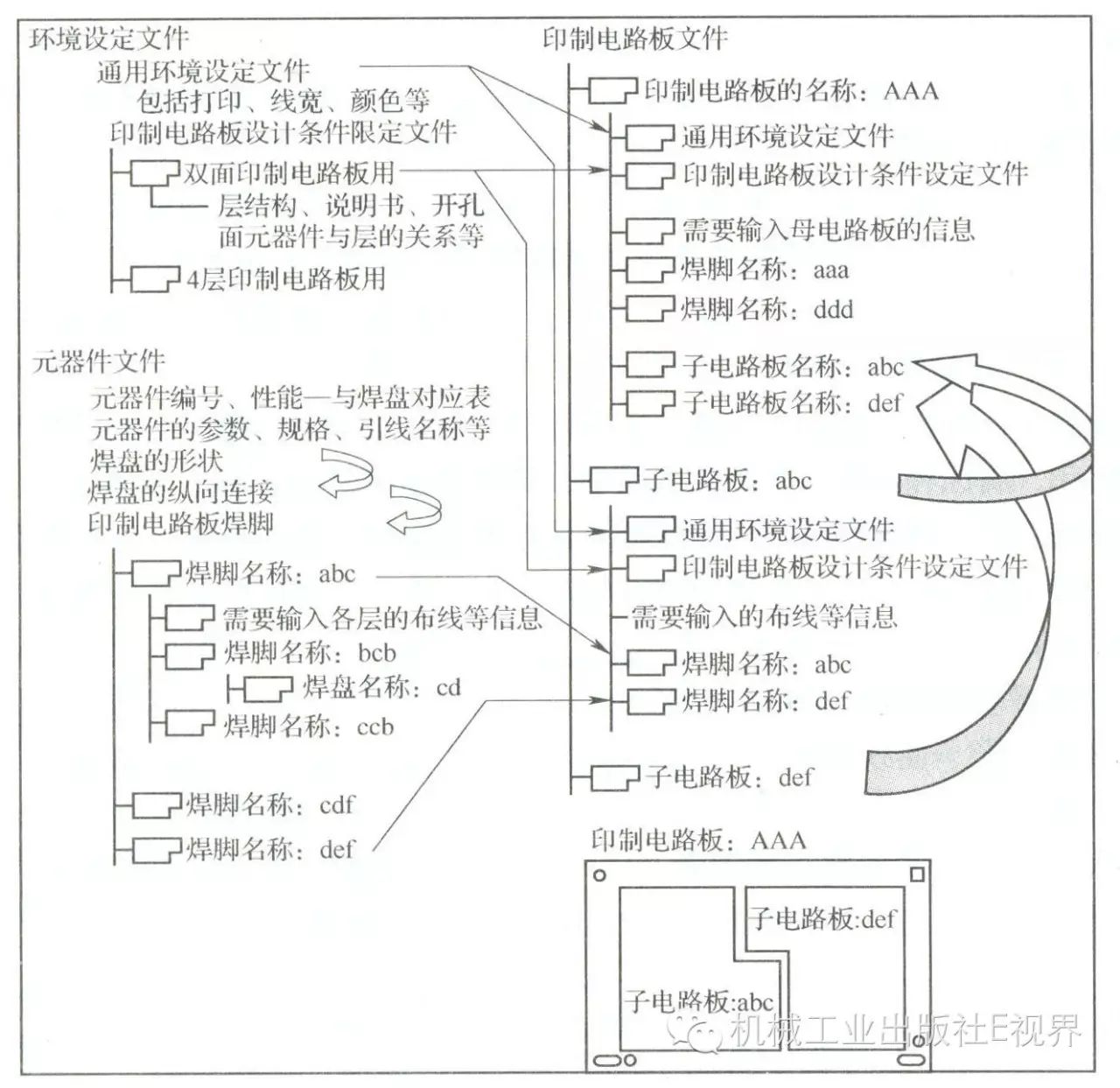 Figure 9 Comparison of Manual Design and Computer-Aided Design
(2) Steps of CAD Operation:
1) Draw the circuit schematic on CAD software.
2) Input parameters that reflect the wiring structure of the printed board into the computer, including pad sizes, component hole sizes and pads, routing relationships, printed wire widths, minimum spacing, and area dimensions for wiring.
3) Execute wiring design commands on the computer, and the computer can automatically complete the design of the printed circuit board.
4) After wiring, review the rationality of the routing and modify any unsatisfactory routes.
5) After finalization, directly draw the black and white background map according to the required scale using a plotter.
6) Save the design to a floppy disk for permanent storage.
(3) Common PCB CAD Software
Currently, the design of printed circuit boards is mostly done using computer design software. Common software includes: SMARTWORK, TANGO, Protel, and others.
Using a computer, the designed PCB diagram can be saved and submitted to the printed circuit board manufacturer.
2
Fabrication and Inspection of Printed Circuit Boards

1.Fabrication of Printed Circuit Boards
The fabrication process of printed circuit boards consists of: base map film production, graphic transfer, etching, mechanical processing of printed circuit boards, and quality inspection.
(1) Base Map Film Production
1) CAD Photographic Method
This method involves using CAD software to route the printed circuit board, then using the obtained data file to drive an optical plotter, exposing the photosensitive film, and creating the original base map film through darkroom operations.
2) Photographic Plate Method
The photographic plate method involves first drawing a black and white base map, then using the drawn black and white base map of the printed circuit board for photographic plate production.
(2) Graphic Transfer
Transferring the printed circuit graphic from the film to the copper-clad board is called graphic transfer.
Specific methods include screen printing and photochemical methods.
1) Screen Printing Method
The screen printing method refers to creating the required printed circuit graphic on a screen, and then using ink to print the graphic onto the copper foil board through the screen template, forming a corrosion-resistant protective layer, which is dried and repaired to achieve graphic transfer.
2) Photochemical Method
Currently, in large-scale production of printed boards, the photochemical method, i.e., direct emulsion production, is mostly used for graphic production. As shown in Figure 10.
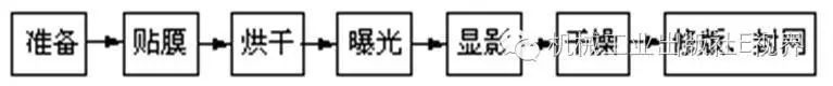 Figure 10 Process Flow of Photochemical Method
(3) Etching Technology (Corrosion)
Etching refers to the process of using chemical or electrochemical methods to remove copper foil from the parts of the printed circuit board that are not exposed after applying the anti-corrosion agent and developing it, leaving precise circuit graphics on the printed board.
Etching methods include shaking tank method, immersion method, and spray etching method.
The shaking tank method is the simplest, using a tank of corrosive agent placed on a continuously shaking platform.
The immersion method involves immersing the workpiece in a large tank that can retain heat for etching.
The spray etching method is faster, using a pump to spray the corrosive agent onto the surface of the printed board for etching processing.
2.Industrial Board Production
In actual production, the manufacturing of printed boards involves dozens of processes. The main ones include:
(1) Drawing the Photographic Base Map
The photographic base map is used to create the photographic master or produce the base plate. Most base maps are drawn by the designer; early printed circuit board production involved manual wiring and pasting, which was inefficient, imprecise, and time-consuming. With the development of computers and their application software, engineering technicians can now use CAD/CAM software to assist in the design and production of printed circuit boards, greatly improving production efficiency and board quality.
(2) Photographic Plate Production
Photographic plate production involves obtaining the original photographic film. The drawn base map is used for photographic plate production, and the plate size should match the PCB size. The production process is similar to ordinary photography and can be divided into soft film cutting→ exposure→ developing→ fixing→ washing→ drying→ repairing.
During plate production, the original image is first enlarged by a certain ratio, and then the enlarged original image is reduced to its original size using microphotography technology, imaging onto light-sensitive materials. After a series of processing steps such as developing, the “original version” or “motherboard” is obtained. Generally, the motherboards are “negative images“.
(3) Graphic Transfer
Transferring the printed circuit graphic from the photographic plate to the copper-clad board is called graphic transfer, which is a very important process in PCB manufacturing. The consistency of the obtained circuit graphic with the desired circuit graphic can be divided into “positive image” and “negative image“.
There are many methods for graphic transfer, with common methods including screen printing and photochemical methods.
1) Screen Printing
Screen printing (abbreviated as silk screen) is an ancient printing process, similar to an oil press. Screen printing involves transferring the printed circuit graphic onto a screen (silk, polyester, etc.) through applying a photosensitive film (film production, exposure, development, film removal) and other photosensitive chemical treatments, creating a hollow graphic. The ink is then pressed onto the copper foil board through a squeegee, resulting in the desired circuit graphic on the copper foil board. These inks are cured with ultraviolet light (or heat) to provide excellent anti-corrosion properties for various applications.
Screen printing uses inks commonly referred to as “anti-corrosion inks,” which come in many varieties, including anti-corrosion inks, electroplating-resistant inks, solder mask inks, character inks, and protective layer inks.
Screen printing can be achieved manually, semi-automatically, or with automatic screen printing machines. Figure 11 shows the simplest screen printing device, where the copper foil board is positioned on the base plate, the printing material is placed in the fixed screen frame, and the printing material is pressed onto the copper foil board to form the desired graphic, which is then dried and repaired.
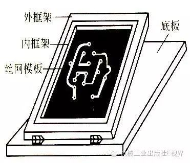 Figure 11 Screen Printing
2) Photochemical Method
The photochemical method includes direct photosensitive methods and photosensitive dry film methods.
① Direct photosensitive method. The process involves surface treatment of the copper-clad board→ applying photosensitive glue→ exposure→ development→ film curing→ repairing. Repairing is a necessary step before etching, allowing for corrections of burrs, broken lines, and pinholes.
② Photosensitive dry film method. The process is similar to the direct photosensitive method, except that a thin film composed of photosensitive polymers (or copolymers), adhesives, photoinitiators, plasticizers, stabilizers, colorants, and solvents is used as the photosensitive material. This film consists of three layers of materials: a polyester film, a photosensitive glue film, and a polyethylene film, with the photosensitive glue film sandwiched in the middle. When using, the outer protective film is removed, and the photosensitive glue film is applied to the copper-clad board using a film applicator.
(4) Etching
Etching, also known as board deterioration, is an important step in the production process, as its success or failure affects subsequent processes in PCB manufacturing. It involves using chemical methods to remove unwanted copper foil from the board, leaving pads, printed wires, and symbols that form the circuit graphic. There are various types of etching agents, with commonly used etching solutions including acidic copper chloride, alkaline copper chloride, and ferric chloride.
Ferric chloride (FeCl3) is widely used as an etching agent in electronics, printed circuits, photographic plate production, and metal finishing. It is suitable for etching copper, copper alloys, Ni-Fe alloys, and steel, especially for etching circuit graphics on printed circuit boards, liquid photosensitive resist, and gold-plated printed circuit boards. The process flow for etching using ferric chloride is as follows:
Pre-etch inspection→ etching→ washing→ acid immersion treatment→ washing→ drying→ removing the anti-corrosion layer→ washing with hot water→ rinsing→ brushing→ drying→ inspection.
Copper chloride (CuCl2·2H2O) is an etching agent that features a simple formula, fast etching speed, high copper dissolution rate, good stability, and ensures product quality, allowing for mechanized continuous production, easy regeneration of solutions, and effective control of environmental pollution. It has rapidly gained popularity in printed circuit board manufacturing and is now the preferred etching agent, replacing ferric chloride.
Copper chloride etching agents are further classified into acidic and alkaline types based on the PCB manufacturing method. Acidic copper chloride etching agents are suitable for screen printing and the production process of inner circuits in multilayer boards, while alkaline copper chloride etching agents are suitable for the production processes of single-sided, double-sided, and multilayer printed outer layer circuits with solder masks (tin-lead).
(5) Metallization of Holes
The metallization of holes lays the foundation for the next step of electroplating to thicken the copper layer and achieve good electrical interconnection. Poor metallization can result in holes lacking copper or having very thin copper layers, leading to open circuits during continuity testing.
Metallized holes are a reliable method for connecting conductive graphics on both sides of double-sided or multilayer boards, and they are one of the most important processes in printed circuit board manufacturing technology. When the wires or pads on both sides of a double-sided printed circuit board need to be interconnected, metallized holes must be used to achieve this. This process is crucial for the internal quality of multilayer boards, mainly involving drilling the required holes, removing drilling debris, and depositing a layer of conductive copper on the walls of the holes, thus metallizing the originally non-metallic walls, also known as copper deposition. This is an essential process in double-sided and multilayer PCBs.
The quality of metallized holes is critical for double-sided PCBs, requiring the metal layer to be uniform, complete, and reliably connected to the copper foil, with electrical and mechanical properties meeting standards. In high-density boards with surface mounting, metallized holes are created using blind hole methods (i.e., copper deposition fills the entire hole) to reduce the area occupied by vias and increase density.
Currently, there are three main types of metallized holes: buried holes, blind holes, and through holes. Buried holes are not visible from the external surface of the substrate, existing within the inner layers of the substrate, created by drilling and plating the holes before lamination. Blind holes can be seen from one outer surface of the substrate, created by laminating first and then drilling holes that do not penetrate through the substrate. Through holes can be seen from both surfaces of the substrate, created by laminating first and then drilling holes that penetrate through the substrate. As shown in Figure 12.
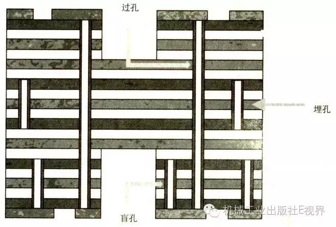 Figure 12 Through Holes, Buried Holes, and Blind Holes in Multilayer Flexible Circuits
“Copper deposition” refers to chemical copper plating, which is a self-catalyzed redox reaction. During chemical copper plating, Cu2+ gains electrons to reduce to metallic copper, while the reducing agent releases electrons and is oxidized. The essence of this reaction is similar to the electrolysis process, except that the electron transfer occurs in a short circuit state, making the current flow invisible externally. Therefore, chemical plating is a highly energy-efficient electrolysis process that does not require an external power supply and has no resistive voltage drop losses during electrolysis. Chemical copper plating can be performed on any non-conductive substrate, and this characteristic has been widely applied in PCB manufacturing, particularly for metallization of holes.
The process flow for metallized holes is as follows:
Drilling the board→ deburring→ removing drilling debris→ cleaning and adjusting treatment→ washing→ roughening→ washing→ pre-immersion→ activating treatment→ washing→ accelerating treatment→ washing→ chemical copper plating→ secondary countercurrent rinsing→ washing→ acid immersion→ electroplating copper thickening→ washing→ drying.
Due to the ecological hazards posed by formaldehyde in chemical copper plating solutions and the potential carcinogenic risks, along with the difficulty of biodegradation of complexing agents (such as EDTA) in chemical copper plating solutions, direct electroplating technology has rapidly developed and been applied in recent years.
(6) Metal Coating
Metal coating involves using chemical and electroplating methods to apply surface coatings on the copper foil of PCBs to improve solderability, electrical conductivity, wear resistance, aesthetics, and to extend the lifespan of PCBs while enhancing electrical reliability. Coating processes are mainly applied to surface-mounted double-sided and multilayer printed circuit boards. Common coating materials include gold, silver, copper, and lead-tin alloys.
1) Copper Plating
Copper plating is one of the fundamental technologies in PCB manufacturing. Copper plating is divided into full-board electroplating (thickening copper after chemical copper plating) and graphic electroplating, where full-board copper plating is performed immediately after chemical copper plating, while graphic electroplating is performed after graphic transfer.
① Full-board electroplating can be used to manufacture printed circuit boards with less strict requirements for width and spacing. The process flow for full-board electroplating is as follows:
Chemical copper plating→ activation→ electroplating copper→ anti-oxidation treatment→ washing→ drying→ brushing the board→ printing negative photoresist patterns→ repairing→ electroplating anti-corrosion metals→ washing→ removing the anti-corrosion agent→ washing→ etching.
② Graphic electroplating is selective electroplating of conductive images. There are generally two scenarios: one method is to first provide a conductive copper layer of 0.5 to 1.0μm through chemical plating, and then perform full-board copper electroplating to achieve a plating thickness of around 5μm.
Graphic copper electroplating is performed after graphic transfer, typically as a base layer for lead-tin or tin plating. In automated production lines, graphic copper electroplating is connected with lead-tin alloy (or tin) electroplating on the same production line. The process flow is as follows:
After graphic transfer of the printed board→ repairing or not repairing→ cleaning treatment→ spraying/washing→ roughening treatment→ spraying/washing→ activation→ graphic copper electroplating→ spraying/washing→ activation→ electroplating lead-tin alloy
└→ Nickel electroplating→ Gold plating
2) Nickel/Gold Plating
To improve wear resistance (during insertion and removal), reduce contact resistance, prevent oxidation (of copper), and enhance connection reliability, nickel and gold plating (commonly referred to as “gold fingers”) are typically applied to PCB connectors and certain special areas. The nickel and gold plating process is usually completed by an automatic production line. The process flow is as follows:
Board loading→ cleaning→ micro-etching→ brushing→ activation→ rinsing→ electroplating→ low-stress nickel plating→ rinsing→ activation→ rinsing→ gold plating→ gold recovery (using)→ rinsing→ drying→ board unloading.
Nickel and gold plating can also be achieved using immersion and chemical plating methods.
3) Tin/Lead Alloy Electroplating
Tin/lead alloy electroplating is mostly performed on automated production lines alongside copper plating. The tin/lead alloy layer serves as an anti-corrosion agent and a solderable layer (after thermal oil melting or infrared melting). Due to the thick layer of tin/lead alloy formed after thermal oil and infrared melting, which is prone to a “tortoise shell” phenomenon, it is unsuitable for surface mount technology. Currently, tin/lead alloy electroplating layers are primarily used as anti-corrosion agents.
4) Chemical Tin Plating
To achieve good soldering performance and meet environmental requirements by eliminating lead content in tin-lead alloys, chemical tin plating is typically used alone.
Tin has good conductivity and solderability. Chemical immersion tin plating on copper substrates involves a displacement reaction between the surface copper layer and tin ions in the tin liquid. Once a tin layer is formed, the reaction immediately stops.
(7) Application of Flux and Solder Mask
After graphic transfer, etching, film removal, and surface metal coating, PCBs should undergo flux or solder mask treatment before assembling components, according to different requirements. Applying flux can improve solderability; on high-density lead-tin alloy boards, to protect the board surface and ensure accurate soldering, a solder mask can be applied to expose the pads while covering other areas under the solder mask.
During soldering, flux can chemically react with various compounds on the surface of the base metal and solder, generating soluble (meltable) compounds. In this process, flux purifies the surfaces of the base metal and solder, preventing the metal surface from oxidizing again.
Solder masking refers to applying a layer of protective ink to all parts except the pads and soldering areas (including graphic wires and substrates). This protective ink prevents bridging between wires during assembly of the completed printed circuit board during “wave soldering,” effectively improving soldering quality and reducing waste. It also saves solder, reduces the weight of the printed circuit board, and lowers costs. Solder mask ink is a permanent coating that does not need to be removed after soldering, providing permanent protection for the printed circuit board.
Solder mask coatings are categorized into thermosetting and photopolymer types, with colors ranging from deep green to light green. The PCB also features text and symbols indicating the positions and names of components, which are typically printed using the screen printing method, commonly in white.
(8) Thermal Melting of Lead-Tin
After electroplating tin-lead on the printed circuit board, the bond between the plating and the copper foil is not strong, and the Sn-Pb alloy plating outside the circuit graphics appears flaky and granular, exhibiting a porous structure that appears dark gray. This can oxidize and discolor during processing and subsequent soldering, affecting solderability. Therefore, it must undergo thermal treatment. This involves heating it above the melting point of the Sn-Pb alloy plating, causing the alloy to re-melt and facilitating the alloy in a molten state to alloy with the base metal, resulting in a dense, shiny, pore-free structure. This process is commonly referred to as “thermal melting.”
Methods for thermal melting of printed circuit boards include infrared melting, thermal oil melting, steam condensation melting, and hot air melting. Currently, infrared melting and thermal oil melting are widely adopted in production. The Sn-Pb alloy is melted using infrared or glycerin baths at temperatures between 190°C and 220°C, ensuring thorough wetting of the copper foil to form a strong bonding layer before cooling.
(9) Hot Air Leveling
Hot air leveling technology has developed rapidly in recent years, combining immersion soldering and hot air leveling. During hot air leveling, the cleaned printed circuit board is first immersed in flux, then dipped into molten solder, and passed between two air knives, where hot compressed air from the air knives melts the tin-lead alloy and blows away excess solder from the printed circuit board. This also removes excess solder from metallized holes, ensuring that no solder accumulates on the surface of printed wires and that holes remain unblocked, resulting in a bright, flat, and uniform solder coating.
(10) Cleaning
Due to various contaminants present during the manufacturing and soldering processes, printed wires and component leads can corrode, leading to short circuits and severely affecting the reliability of printed circuits. Therefore, strict cleaning of various printed circuits and printed circuit assemblies (PCA) is essential to remove residues of flux, anti-oxidation oils, solder contaminants, and other pollutants, especially residues of flux. Generally, the cleanliness of printed circuit boards after cleaning should meet the MIL-P-28809 standard.
Common cleaning agents include fluorocarbon cleaning agents, and the main process methods are: gas washing – spraying – gas washing – drying.
Due to the environmental hazards posed by fluorocarbon solvents, various countries are considering new materials and technologies to replace fluorocarbon solvents for cleaning. At the same time, no-clean technology is gradually being promoted. The realization of no-clean processes can be achieved through two methods: one is using low-solid soldering agents, and the other is soldering in inert gases.
3.Quality Inspection of Printed Circuit Boards
After completing mechanical processing, quality inspection of printed circuit boards should be conducted. The main inspection items include visual inspection, continuity testing, insulation resistance testing, and solderability testing.
(1) Visual Inspection
Visual inspection refers to checking visible conditions with the naked eye. Typically, visual inspection can identify some obvious surface defects, such as whether wires are intact, whether pad sizes are appropriate, and whether solder holes are centered on pads.
(2) Continuity Testing
Continuity testing should be performed on multilayer circuit boards to determine whether the printed circuit graphics are connected. This test can be conducted using a multimeter.
(3) Insulation Resistance Testing
Measuring the resistance of insulating components of printed circuit boards against applied DC voltage is referred to as insulation resistance.
In printed board circuits, this test can be performed between wires on the same layer or between two different layers.
(4) Solderability Testing
Solderability testing measures the ability of solder to adhere to the printed graphics when components are connected to the printed board. Solderability is generally indicated as adherent, semi-adherent, or non-adherent.
(-END-)
Excerpt from “Technology and Assembly of Electronic Products”
 The Mechanical Industry Press E-World Bookstore is now online!
Click the “Preface Hotspots” menu → “Bookstore” to purchase!
Previous Highlights
Common Knowledge in Electronics: What is the Limit Temperature of Chips?
Basic Knowledge of LEDs: LED Light Emission Principles, Packaging Forms, Technical Indicators, and Precautions
Knowledge Essential for Mastering Electronic Technology: Disassembly and Soldering of Components