Source | AUTO GenerationAuthor | AUTO GENERATIONAs automotive electronic control systems gradually develop towards centralization, the complexity of software continues to increase. Chips, as the core carriers of automotive electrification and intelligence, are becoming increasingly significant.For autonomous driving systems, the realization of technology relies on the real-time processing of a large amount of sensor data, requiring deep learning and machine learning algorithms to ensure that this data is processed and analyzed in a very short time, allowing vehicles to make timely and accurate decisions. This not only requires chips to have super strong computing power and high-speed data processing capabilities but also low latency and high reliability and safety to ensure driving safety.
I have always believed that as automotive R&D engineers, whether engaged in system or software development, knowledge of hardware or chips is crucial for understanding systems and software. Especially when we look beyond the surface and delve into the essence, a systematic knowledge structure is particularly important.To this end, I have specifically opened a new series of articles on automotive chip systems, starting from the basics of chip content and gradually elaborating on automotive chip-related topics.
When talking about automotive chips or automotive control units, many friends may immediately think of the following concepts: CPU (Central Processing Unit), MCU (Microcontroller Unit), GPU (Graphics Processing Unit), SoC (System on Chip), SBC (System Basis Chip), etc.
But what are the essential differences between them, and what are their respective functions, architectures, and application scenarios? Therefore, taking the opening article of the chip series as an opportunity, today I will first explain the basic chip concepts of CPU, MCU, and SBC to my friends, and we will discuss the remaining GPU and SoC related content in the next article!
01
CPU and Von Neumann Architecture
When talking about CPU (Central Processing Unit), we must mention the pioneer of modern computer design, the Von Neumann architecture, which is a computer architecture model proposed by mathematician and physicist John von Neumann in the 1940s and serves as the foundation of modern computer design.
So what is the relationship between the Von Neumann architecture and the CPU?
The core idea of the Von Neumann architecture is to store program instructions and data in the same memory space and transmit them through a single system bus.
This idea seems self-evident now, but it had a revolutionary impact on computer systems at the time. In the early computers, program instructions and data were treated as independent entities, with program instructions being fixed as part of the controller hardware, non-reprogrammable, meaning a computer could only execute a specific program, which meant a strong binding between hardware and programs, resulting in very low flexibility. The emergence of the Von Neumann architecture completely changed this phenomenon, directly promoting the separation of software and hardware design in computer systems, decoupling hardware, and thus the pure programmer was born !
!
According to the Von Neumann architecture, as shown in the figure below, a computer structure consists of five main components:
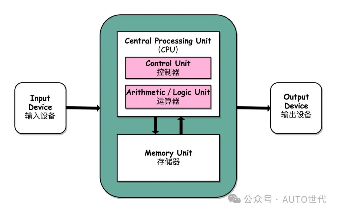 ─ Arithmetic/Logic Unit (ALU): Completes various arithmetic and logical operations. The main function of the ALU is to perform arithmetic operations such as addition, subtraction, multiplication, and division, as well as logical operations such as AND, OR, NOT, XOR, and shift operations under the influence of control signals.
─ Control Unit(CU): Directs the orderly operation of the ALU, including fetching instructions from memory, translating instructions, analyzing instructions, and then sending control commands to relevant components based on the instructions to execute the operations contained in the instructions.
─ Memory Unit(MU): A hardware component used to store data and program instructions, which can be further divided into internal memory, external memory, random access memory (RAM), and read-only memory (ROM), etc., based on their location and characteristics.
─ Input/Output Device: Used to interact with the external environment, such as keyboards, mice, monitors, etc.
Among these, the ALU and control unit are integrated within the CPU, thus giving birth to the CPU.
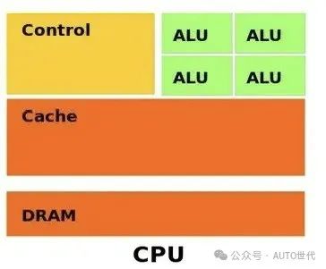
Since the CPU must possess extremely high versatility to handle various data types and perform logical judgments, this introduces a large number of branch jumps and interrupt handling, making the internal structure of the CPU exceptionally complex. It is precisely because of this that the number of ALU units inside the CPU is actually very limited, with most of the space occupied by the control unit and cache. To increase the possibility of parallel computing, the CPU can adopt a multi-core structure, such as dual-core, quad-core, or six-core, but the number will not be too many!
In the CPU memory system, there is an important concept called cache, which is used to reduce the time required for the CPU to access DRAM. Cache is a smaller memory area but with faster access speed, located closer to the processor core, used to store copies of data from DRAM. Cache is usually divided into multiple levels, typically including three levels: L1, L2, and L3. The closer the cache is to the core, the smaller its capacity but the faster its speed. For example, L1 cache may be 64KB, L2 cache is 256KB, and L3 cache is 4MB.
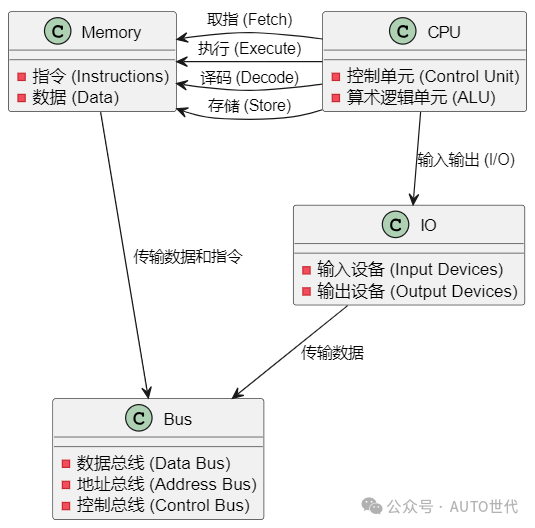
The basic workflow is shown in the figure below:
In addition, to increase computational efficiency, the CPU adopts a MIMD (Multiple Instruction, Multiple Data) working mechanism. Simply put, MIMD is like various departments in a large company, where each department (processor) independently handles different tasks (instructions) and data, improving overall efficiency through parallel work. This mechanism allows the system to handle multiple tasks simultaneously, flexibly responding to different needs, but it also requires effective management to coordinate resources and tasks, ensuring that all work proceeds smoothly.
However, as the demand for computing speed increases, the Von Neumann architecture has gradually encountered bottlenecks:
1. Von Neumann Bottleneck: Due to the sharing of the same bus for instructions and data, the CPU needs to use the same bus for each read of instructions and data, causing performance bottlenecks.
2. Memory Speed Limitations: While CPU speeds continue to increase, memory speeds are relatively slow, leading to an increasing amount of time the CPU spends waiting for memory responses.To alleviate the Von Neumann bottleneck, especially with the rise of AI and machine learning, the CPU spends most of its time waiting for data to be transferred from memory to the calculator. This process not only reduces computational efficiency but also consumes a lot of energy. Therefore, modern computer technology has adopted many technical measures, such as using different levels (e.g., L1, L2, L3) of cache or “near-memory” architectures, making memory elements closer to logic units, or even integrating memory and computation architectures. Of course, this also involves GPU-related content, which we will discuss in detail in the next article. Friends can just have a concept for now.
02
MCU: Automotive Embedded Solutions
MCU (Microcontroller Unit) is a microcontroller that integrates various functional modules such as CPU, memory (ROM/RAM), data converters (A/D, D/A), input/output interfaces (I/O), and timers.
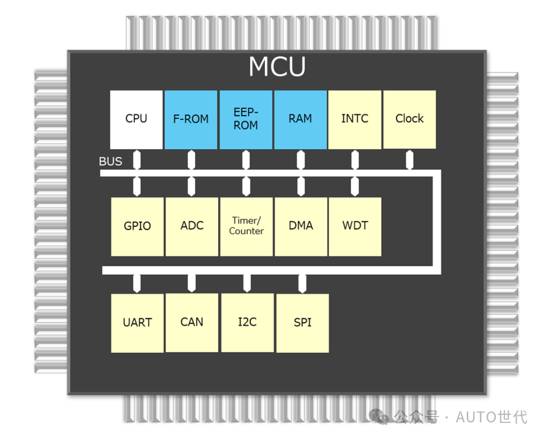
Compared to the PC processors that most people are familiar with, the MCU has appropriately reduced specifications and frequencies to meet the strict requirements of computing control devices regarding space, power consumption, real-time performance, cost, or safety. Therefore, in the automotive controller field, it is also referred to as automotive-grade embedded MCU, mainly used for control units of automotive components or integrated domains, such as vehicle dynamics, power batteries, body control, safety systems (e.g., ABS, ESP, etc.), and advanced driver assistance systems.Depending on the requirements, MCU chips can be divided into 8-bit, 16-bit, and 32-bit, where “bit” refers to the “bit width” of the MCU, indicating the number of binary bits that a single instruction can process. Theoretically, the larger the MCU bit number, the larger the amount of data processed at one time, the faster the processing speed, and the stronger the performance.Currently, 8-bit MCUs dominate the market due to their simple design and cost advantages, while 32-bit MCUs dominate due to their good performance, with the 16-bit MCU market being increasingly squeezed.Currently, the development of automotive-grade MCUs is still mainly monopolized by foreign suppliers. Although some alternative solutions have emerged domestically, their market share remains relatively low.So where exactly does embedded MCU development face challenges?1. High Reliability and Durability: Automotive-grade MCUs must be able to operate reliably under harsh environmental conditions, including extreme temperatures, humidity, vibration, and electromagnetic interference. They typically need to pass strict AEC-Q100 standard certification to ensure their stability and longevity in practical applications.
2. High Performance and Low Power Consumption: With the increase in automotive electronic functions, MCUs need to process more data and perform more complex computational tasks. Therefore, automotive-grade MCUs need to have high-performance computing capabilities while also controlling power consumption to meet the demands of automotive battery power supply.
3. Safety: To ensure driving safety, automotive-grade MCUs must comply with functional safety standards such as ISO 26262, possessing multiple safety protection mechanisms, including hardware security modules (HSM), supporting encryption algorithms, and secure boot functions to prevent hacking and data tampering.
4. Real-time Performance: In autonomous driving and advanced driver assistance systems (ADAS), MCUs need to respond in real-time to various sensor data and make decisions. Therefore, automotive-grade MCUs typically need to have strong real-time processing capabilities and low latency performance.
In addition, to achieve hard real-time, high reliability, and safety in automotive control systems, and to make software development and integration on different MCU platforms more efficient and portable, AUTOSAR (Automotive Open System Architecture) was born, which is also a unique product of automotive MCUs.
AUTOSAR introduces a hardware abstraction layer, allowing upper-layer software to be independent of specific MCU hardware, and through standardized interfaces and services, AUTOSAR enables application software to run on different MCU platforms, requiring only adaptation of the underlying drivers. However, it is still largely monopolized by foreign entities, and the cost of development toolchains is extremely high. Although more and more non-AUTOSAR software architectures are being applied to intelligent driving systems, AUTOSAR still holds an unshakable position in traditional hard real-time and high safety requirement control systems!
03
SBC: Safety Monitoring Solutions
System Basis Chip (SBC) is an independent chip that integrates functions such as power management, communication interfaces, monitoring diagnostics, and safety monitoring.The design intention of SBC is to provide an efficient and low-cost solution for specific functions. It can power sensors, perform data communication, or provide external independent watchdog services, clocks, etc. Compared to a complete microcontroller (MCU), SBC reduces costs through streamlined design, focusing on providing specific functions, thus can essentially be seen as a simplified version of an MCU optimized for specific application scenarios.For example, the NXP FS86 basis chip has the following structure: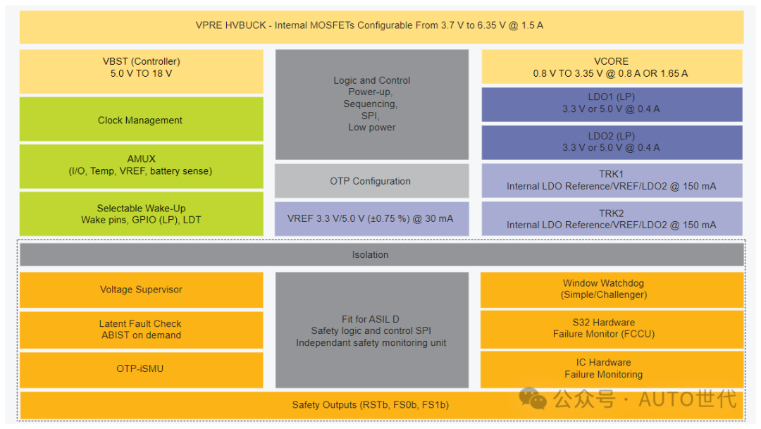 Among them, FS26 has multiple switch-mode regulators and LDO regulators to power microcontrollers, sensors, peripheral ICs, and communication interfaces. FS26 provides high-precision voltage references for the system and reference voltages for two independent voltage tracking regulators. In addition, it offers various functions for system control and diagnostics, such as analog multiplexers, GPIOs, optional I/O wake-up events, long-duration timers, or SPI communication.FS26 complies with ISO 26262 standards, covering ASIL B and ASIL D safety integrity levels. It has multiple fault-safe outputs, becoming an integral part of safety-oriented system partitions, and features the latest on-demand potential fault monitoring capabilities, such as error handling during startup (e.g., logic built-in self-test (LBIST), memory built-in self-test (MBIST)), Software Watchdog Timer (WDT), Memory Protection Unit (MPU), etc.
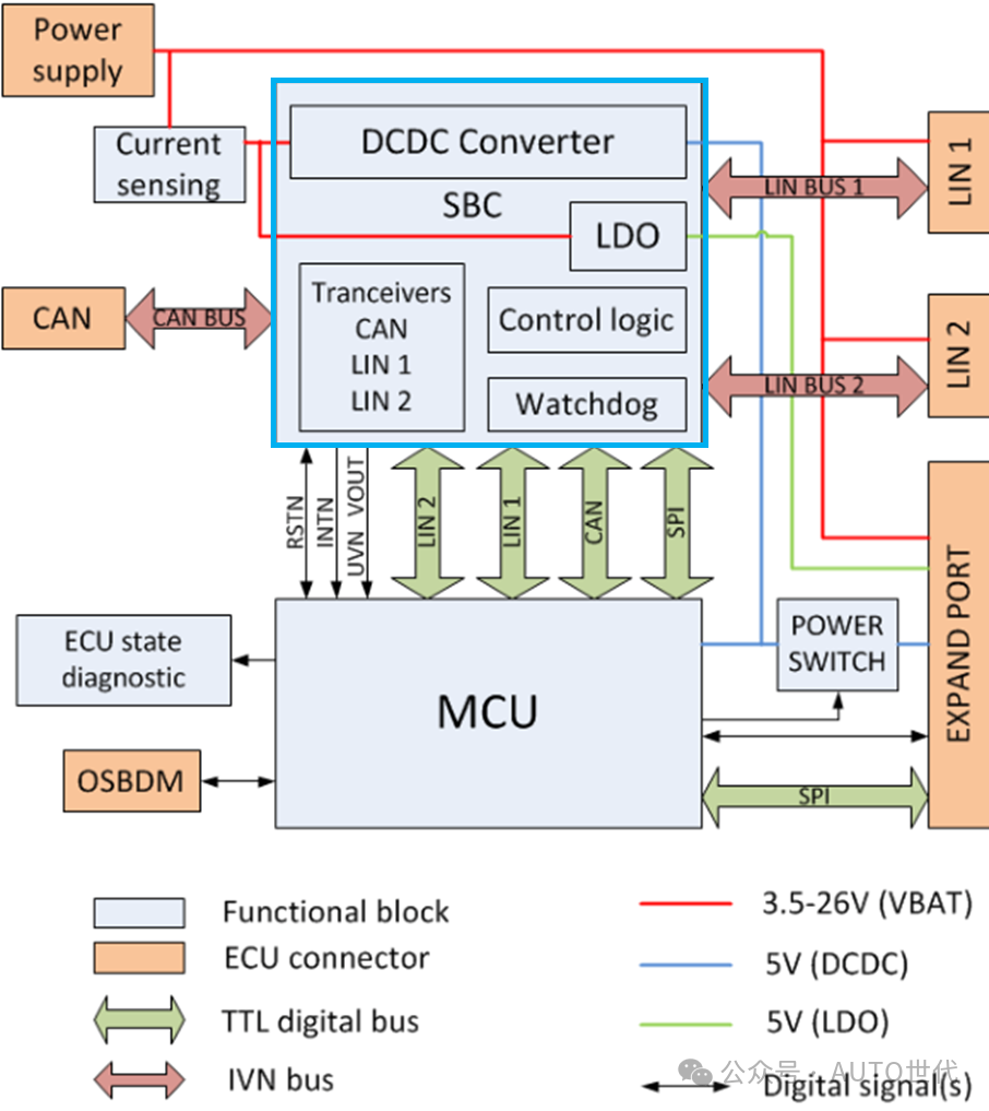
Therefore, in functional safety monitoring architectures, including the classic three-layer E-Gas architecture, SBC chips are often used as independent monitoring chips to monitor the main MCU and provide watchdog, interrupt, and other services, as shown in the figure below:
In Conclusion:
We have completed our discussion on the chip series, decoding automotive processors CPU, MCU, and SBC related content. I hope it can provide friends with a better understanding.
-END-This article is for educational exchange purposes only and does not constitute any investment advice. Some images are sourced from the internet and copyright ownership has not been verified. It is not for commercial use. If there are any infringements, please contact us at [email protected].