Word count: 1092, reading time approximately 6 minutes
Continuing from the last session, today we will implement the functionality of UART, primarily using the hardware description language Verilog.
The interface design is actually quite simple. If we distill its essence, it can be divided into three main parts: data acquisition, state machine, and interface timing. As long as these three steps are done well, most chip interface designs are quite similar. The only considerations are whether data acquisition needs to account for competition with other interfaces, the complexity of the protocols in the state machine, and the transition from single-line to multi-line interface timing.
1 Data Acquisition
The data acquisition step generally involves retrieving data from the chip’s memory. Referring back to the previous section on creating your own chip (Part 1), the interface is analogous to the external organs of a human body, which exchange information with the outside world, sourced from other organs or the brain (analogous to speaking, which requires the brain to organize language). However, this process requires the involvement of a bus to transport data to the interface. Here, we will start with a simple interface protocol and gradually incorporate bus protocols like APB and AHB.Now, we define the protocol as shown in the figure below:
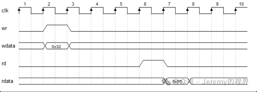
A write signal (wr) will write the data 0x32 received by UART into the chip’s memory, and a read signal (rd) will allow UART to retrieve the data 0x55 from the chip’s memory in the next cycle. Our UART interface will follow this protocol to exchange data with the chip’s memory.
2 State Machine
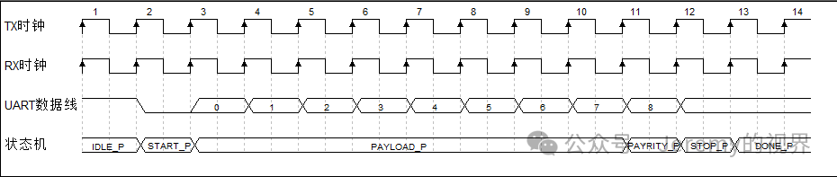
The state machine is not exactly a design technique within the chip; rather, it is a universal concept. As the name suggests, a state machine involves state transitions. To illustrate this concept with a simple example, consider our daily routine, which may resemble that of a robot: waking up -> brushing teeth -> having breakfast -> driving to work -> working -> lunch -> working -> returning home -> showering and sleeping. Each day, we may continuously transition between these states. The state machine in a chip operates on a similar structure, utilizing MUX (multiplexers) and COUNTERs to construct the state machine.First, we define the states:
localparam IDLE_P    = 3'd0; // Idle state
localparam START_P   = 3'd1; // Start bit
localparam PAYLOAD_P = 3'd2; // Data bit
localparam PARITY_P  = 3'd3; // Parity bit
localparam STOP_P    = 3'd4; // Stop bit
localparam DONE_P    = 3'd5; // End of transmission or reception
Next, we expand the diagram from the previous section, which will become:
The implementation code is as follows:
always @(posedge clk or negedge rstn) begin
    if(~rstn) begin
        uart_stm    <= #UDLY IDLE_P;
    end
    else begin
        uart_stm    <= #UDLY uart_nxt_stm;
    end
end

always @(*) begin
    case(uart_stm)
        IDLE_P    :
        begin
            if(idle_st)
                uart_nxt_stm = START_P;
            else
                uart_nxt_stm = IDLE_P;
        end

        START_P   :
        begin
            if(start_done)
                uart_nxt_stm = PAYLOAD_P;
            else
                uart_nxt_stm = START_P;
        end

        PAYLOAD_P :
        begin
            if(payload_done)
                uart_nxt_stm = PARITY_P;
            else
                uart_nxt_stm = PAYLOAD_P;
        end

        PARITY_P  :
        begin
            if(parity_done)
                uart_nxt_stm = STOP_P;
            else
                uart_nxt_stm = PARITY_P;
        end

        STOP_P    :
        begin
            if(stop_done)
                uart_nxt_stm = DONE_P;
            else
                uart_nxt_stm = STOP_P;
        end

        DONE_P    :
        begin
            uart_nxt_stm = IDLE_P;
        end

        default : uart_nxt_stm = IDLE_P;
    endcase
end
3 Interface Timing
Now we move to the final step, interface timing. After designing the state machine, there is not much to consider regarding interface timing during reception, as the sender controls the interface timing. We only need to ensure that the state machine operates correctly. The key concern now is the control of transmission, as UART is a simple asynchronous serial interface with only one line. Therefore, we only need to control the output data line according to the timing diagram.The code is as follows:
//******************************//
//       output interface       //
//******************************//
wire uart_tx_in;
wire start_pls;
wire payload_pls;
wire parity_pls;
wire stop_pls;

assign start_pls   = idle_st;
assign payload_pls = start_done | (s_payload & div_cnt_clr & ~payload_done);
assign parity_pls  = payload_done;
assign stop_pls    = parity_done;

assign uart_tx_in = start_pls   ? 1'b0         :
                    payload_pls ? uart_buf[00] :
                    parity_pls  ? parity       :
                    stop_pls    ? 1'b1         : uart_tx;

always @(posedge clk or negedge rstn) begin
    if(~rstn) begin
        uart_tx <= #UDLY 1'b1;
    end
    else begin
        uart_tx <= #UDLY uart_tx_in;
    end
end
4 Conclusion
We have successfully designed a simple UART module. The code presented above is the core code, and due to space limitations, some details are not elaborated here. You can also try designing a UART on your own.
5 Upcoming Topics
In the future, I plan to introduce the IIS interface and audio ADDA interface, and then design an NPU, aiming to create a chip that incorporates AI for audio processing! Let’s work hard together!!!
Feel free to add me on WeChat: Jeremy3141592654 for discussions, and don’t forget to follow!
Previous Articles
In 1997, at 28 years old, where should IC engineers go?
Common debugging techniques for IC designers