In today’s low-end digital communication applications, we frequently encounter IIC (Inter-Integrated Circuit) and SPI (Serial Peripheral Interface). The reason is that these two communication protocols are very suitable for short-distance, low-speed communication between chips. Philips (for IIC) and Motorola (for SPI) developed these two standard communication protocols based on different backgrounds and market needs.
IIC was developed in 1982 to provide a simpler interconnection method for CPUs and peripheral chips in televisions. Televisions were among the earliest embedded systems, and the initial embedded systems used memory-mapped I/O to interconnect microcontrollers and peripheral devices. To achieve memory mapping, devices had to be connected in parallel to the microcontroller’s data and address lines, which required a large number of lines and additional address decoding chips, making it inconvenient and costly.
To save microcontroller pins and additional logic chips, simplifying the printed circuit board and reducing costs, Philips laboratories in the Netherlands developed the “Inter-Integrated Circuit,” IIC or I2C, a bus protocol that connects all peripheral chips using only two wires. The initial standard defined a bus speed of 100 kbps. After several revisions, the speeds were updated to 400 kbps in 1995 and 3.4 Mbps in 1998.
There are indications that the SPI bus was first introduced in 1979, with Motorola integrating the SPI bus into their first microcontroller chip modified from the 68000 microprocessor. The SPI bus is an external bus for microcontrollers with four lines (as opposed to an internal bus). Unlike IIC, SPI does not have a formal standard; it is merely a de facto standard that provides a general abstract description of the communication operations, with chip manufacturers and driver developers communicating implementation details through data sheets and application notes.
Introduction to SPI Bus
For experienced digital electronic engineers, interconnecting two digital devices using SPI is quite intuitive. SPI is a four-signal line protocol, as shown in the diagram below.
-
SCLK: Serial Clock (output from master).
-
MOSI; SIMO: Master Output, Slave Input (output from master).
-
MISO; SOMI: Master Input, Slave Output (output from slave).
-
SS: Slave Select (active low, output from master).
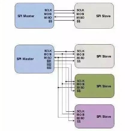
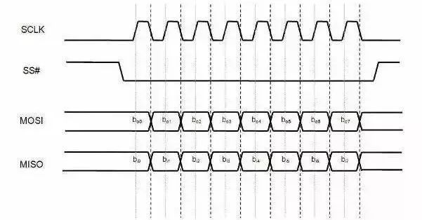
SPI is a single-master communication protocol, meaning that only one central device in the bus can initiate communication. When the SPI master device wants to read/write from/to a slave device, it first pulls down the corresponding SS line of the slave device (SS is active low), then begins sending working pulses to the clock line. At the corresponding pulse time, the master device sends signals to MOSI to achieve “write,” while it can sample MISO to achieve “read,” as shown in the diagram below.
SPI has four operating modes: Mode 0, Mode 1, Mode 2, and Mode 3. The differences lie in which edge of the clock pulse toggles the output signal, which edge samples the input signal, and the stable level of the clock pulse (whether the clock signal is high or low when inactive). Each mode is characterized by a pair of parameters known as clock polarity (CPOL) and clock phase (CPHA).
The master and slave devices must use the same working parameters—SCLK, CPOL, and CPHA—to function correctly. If there are multiple slave devices using different working parameters, the master device must reconfigure these parameters when reading/writing different slave devices.
SPI does not specify a maximum transmission rate, nor does it have an addressing scheme; it also does not define a communication acknowledgment mechanism or flow control rules. In fact, the SPI master device does not even know whether the specified slave device exists. All these communication controls must be implemented outside the SPI protocol. For example, to connect a “command-response control” decoding chip using SPI, a more advanced communication protocol must be implemented on top of SPI.
SPI does not concern itself with the electrical characteristics of the physical interface, such as signal standard voltages. Initially, most SPI applications used intermittent clock pulses and transmitted data in bytes, but now many variants have implemented continuous time pulses and arbitrary-length data frames.
Introduction to IIC Bus
Unlike the single-master nature of SPI, IIC is a multi-master bus that does not have physical chip select signal lines or arbitration logic circuits, using only two signal lines—serial data (SDA) and serial clock (SCL).
The IIC protocol specifies:
-
Each IIC device has a unique seven-bit device address.
-
The data frame size is an 8-bit byte.
-
Some data bits in the data (frame) are used to control the start, stop, direction (read/write), and acknowledgment mechanisms of the communication.
The IIC data transmission rates include standard mode (100 kbps), fast mode (400 kbps), and high-speed mode (3.4 Mbps), with some variants implementing low-speed mode (10 kbps) and fast+ mode (1 Mbps).
Physically, the IIC bus consists of two signal lines and one ground line. Both signal lines are bidirectional, as shown in the diagram below. The IIC protocol standard specifies that the device initiating communication is called the master device, and after the master device initiates a communication, all other devices are considered slave devices.

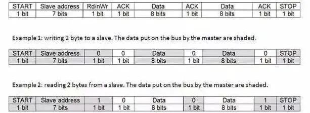
The IIC communication process is roughly as follows. First, the master device sends a START signal, which is like shouting to all other devices: “Please pay attention!” Then, other devices begin to listen to the bus in preparation to receive data. Next, the master device sends a 7-bit device address along with a read/write operation data frame. When the device receives the data, it compares the address to see if it is the target device. If the comparison does not match, the device enters a waiting state until the STOP signal arrives; if it matches, the device sends an acknowledgment signal—ACKNOWLEDGE in response.
Once the master device receives the acknowledgment, it begins to send or receive data. The data frame size is 8 bits, followed by an acknowledgment signal. The master device sends data, and the slave responds; conversely, when the master device receives data, it acknowledges. When the data transfer is complete, the master device sends a STOP signal to announce the release of the bus, and other devices return to their initial state.
Based on the physical structure of the IIC bus, the START and STOP signals on the bus must be unique. Additionally, the IIC bus standard specifies that the data transitions on the SDA line must occur during the low period of the SCL line, and during the high period of the SCL line, the SDA line data must be stable.
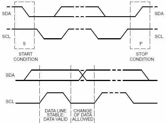
In physical implementation, both the SCL and SDA lines are open-drain, connected to a voltage source through pull-up resistors. When the line is grounded, it represents logic 0; when the line is released and idle, it represents logic 1. Based on these characteristics, IIC devices can only operate on the bus by “pulling the line low”—outputting logic 0.
The IIC bus design uses only two lines but elegantly achieves seamless communication among any number of devices, making it a perfect solution. Let’s imagine what would happen if two devices simultaneously sent information to the SCL and SDA lines.
Based on the design of the IIC bus, there can be no level conflict on the line. If one device sends logic 0 while another sends logic 1, the line will only see logic 0. In other words, if a level conflict occurs, the device sending logic 0 always “wins.”
The physical structure of the bus also allows the master device to write data to the bus while reading data. This way, any device can detect the occurrence of a conflict. When two master devices compete for the bus, the “winner” does not know about the competition; only the “loser” discovers the conflict—when it writes a logic 1 but reads 0—and withdraws from the competition.
Ten-Bit Device Address
Each IIC device has a 7-bit address, theoretically allowing for only 127 different IIC devices. In reality, there are far more types of IIC devices than this limit, and the probability of having IIC devices with the same address on a single bus is quite high. To overcome this limitation, many devices use dual addressing—7-bit address plus pin address (external configuration pins). The IIC standard also anticipated this limitation and proposed a 10-bit addressing scheme.
The 10-bit addressing scheme impacts the IIC protocol in two ways:
First, the address frame is two bytes long, whereas it was originally one byte.
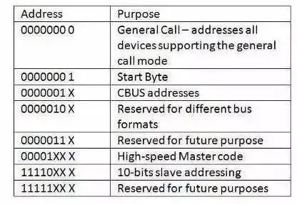
Second, the first five bits of the first byte are used as the 10-bit address identifier, designated as “11110.”
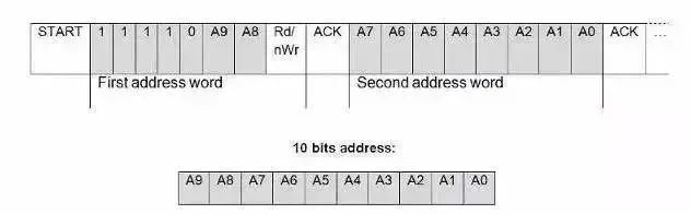
In addition to the 10-bit address identifier, the standard also reserves some address codes for other purposes, as shown in the table below:
Clock Stretching
In IIC communication, the master device determines the clock speed, as the clock pulse signal is explicitly generated by the master device. However, when the slave device cannot keep up with the master device’s speed, it needs a mechanism to request the master device to slow down, known as clock stretching. Due to the special structure of IIC, this mechanism is implemented. When the slave device needs to reduce the transmission speed, it can pull down the clock line, forcing the master device into a wait state until the slave device releases the clock line, at which point communication continues.
High-Speed Mode
In principle, using pull-up resistors to set logic 1 limits the maximum transmission speed of the bus. Speed is one of the factors that restrict bus applications. This explains why high-speed mode (3.4 Mbps) was introduced. Before initiating a high-speed mode transmission, the master device must first send a specific “High Speed Master” signal in a lower-speed mode (e.g., fast mode). To shorten the signal period and increase bus speed, high-speed mode must use additional I/O buffers. Additionally, bus arbitration can be masked in high-speed mode. For more information, please refer to the bus standard documentation.
Comparison of IIC and SPI
Let’s compare some key points between IIC and SPI.
1. Bus Topology Structure / Signal Routing / Hardware Resource Consumption
IIC requires only two signal lines, while standard SPI requires at least four signal lines, and more if there are multiple slave devices. Some SPI variants use only three lines—SCLK, SS, and bidirectional MISO/MOSI—but the SS line still needs to be one-to-one with each slave device. Additionally, if SPI is to implement a multi-master structure, the bus system requires extra logic and lines. The only issue with building a system bus using IIC is the limited 7-bit address space, but this problem has been addressed by the new standard—using 10-bit addresses. From this first point, IIC is clearly the big winner.
2. Data Throughput / Transmission Speed
If high-speed data transmission is a must in the application, then SPI is the obvious choice. This is because SPI is full-duplex, while IIC is not. SPI does not define speed limits, and typical implementations can reach or even exceed 10 Mbps. The highest speed for IIC is only the fast+ mode (1 Mbps) and high-speed mode (3.4 Mbps), with the latter requiring additional I/O buffers, which are not always easy to implement.
3. Elegance
IIC is often considered more elegant than SPI. Fairly speaking, the author tends to believe that both are equally elegant and robust. The elegance of IIC lies in its features—achieving multi-master arbitration and device routing with a lightweight architecture. However, for engineers using it, understanding the bus structure can be more challenging, and the bus performance is not high.
The advantage of SPI lies in its structure being quite intuitive and simple, easy to implement, and having good scalability. The simplicity of SPI does not necessarily make it elegant, as building a useful communication platform with SPI requires constructing specific communication protocol software on top of SPI. In other words, to gain the high-speed performance unique to SPI that IIC lacks, engineers need to invest more effort. Moreover, this custom work is entirely freeform, which explains why SPI does not have an official standard. Both IIC and SPI provide good support for low-speed device communication; however, SPI is suitable for data stream applications, while IIC is more suited for multi-master applications with “byte devices.”
Conclusion
In the cluster of digital communication protocols, IIC and SPI are often referred to as “small” protocols, in contrast to Ethernet, USB, SATA, PCI-Express, and other buses that achieve transmission speeds of hundreds to thousands of gigabytes per second. However, we must not forget the purpose of various buses. “Large” protocols are used for communication between entire systems outside the system, while “small” protocols are used for communication between chips within the system. There is no indication that “large” protocols need to replace “small” protocols. The existence and popularity of IIC and SPI reflect the philosophy of “good enough is sufficient.” In response to the opening statement, the popularity of IIC and SPI makes them essential tools for any embedded engineer.