01classProject OverviewProject 12 Digital Thermometer Design
Project 13 Application of AT24C04
Project 14 Application of Real-Time Clock DS1302
Project 15-1 Application of A-D Converter ADC0832
Project 15-2 Application of A-D Converter TLC549
Project 16 Application of D-A Converter TLC5615
Project 17 Application of Driver ULN2003
Due to the large amount of content, this article only introduces three project examples. The complete content is recommended for download, and the download method will be provided at the end of the article.
02classApplication of A-D Converter ADC08321. Functional Principle
ADC0832 is an 8-bit successive approximation CMOS dual-channel A-D converter produced by National Semiconductor. This device is available in 8-pin and 14-pin packages, powered by a 5V supply, with an analog voltage input range of 0~5V and an internal clock of 250kHz, achieving a conversion speed of 32μs. The package diagram is shown in Figure 7.
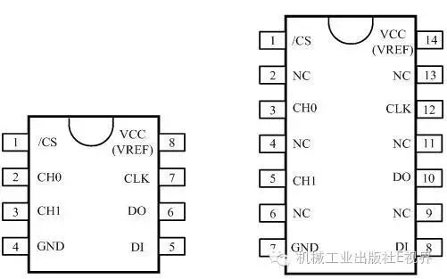 Figure 7 ADC0832 Package
Since ADC0832 uses serial communication, it occupies fewer MCU I/O resources and is generally used in simple analog voltage detection systems. The pin functions are shown in Table 1.
Table 1 ADC0832 Pin Functions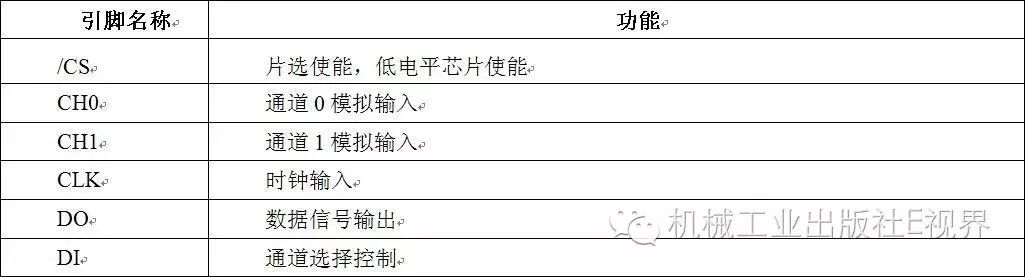
Connecting ADC0832 to the MCU requires 4 signal lines: /CS, CLK, DO, and DI. Since the DO and DI terminals are not simultaneously active during communication and the interface with the MCU is bidirectional, in applications, the DO and DI lines of ADC0832 can be connected together to the MCU’s I/O. As shown in Figure 8.
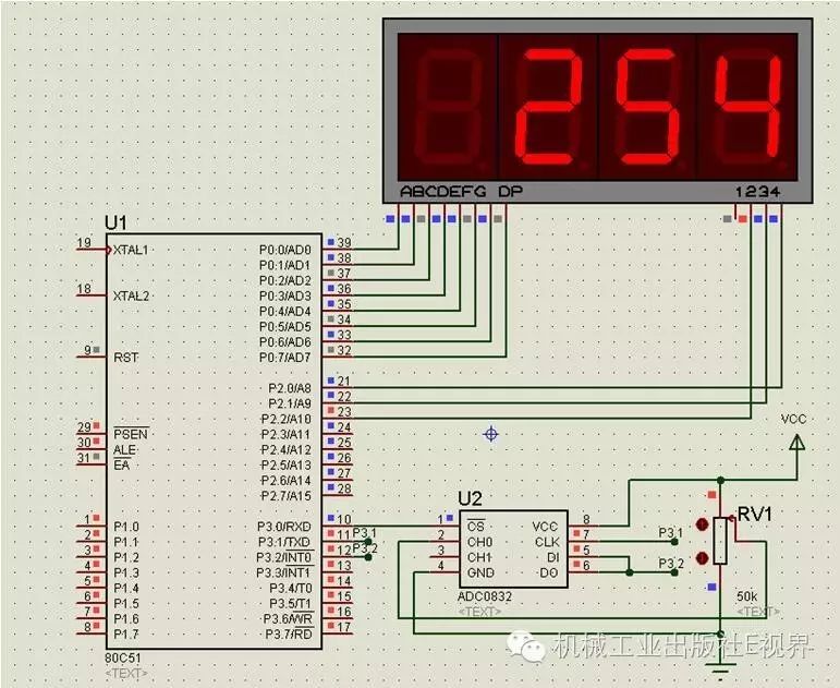 Figure 8 ADC0832 Simulation Circuit
When ADC0832 is not working, the /CS terminal should be high, at which point the chip is disabled, and the levels of CLK and DO/DI can be arbitrary. To perform an A-D conversion, the enable terminal /CS must first be set to low and kept low until the conversion is completely finished. When starting the conversion, the MCU sends clock pulses to the CLK input of ADC0832, and the DO/DI terminal uses the signal selected by the input channel function. On the falling edge of the first clock pulse, the DI terminal must be high to indicate the start signal. On the falling edges of the 2nd and 3rd clock pulses, the DI terminal should input two bits of data to select the channel. If these two bits are 1 and 0, only CH0 will perform single-channel conversion; if both bits are 1, only CH1 will perform single-channel conversion; if both bits are 0, CH0 will be the positive input IN+ and CH1 will be the negative input IN-; if the bits are 0 and 1, CH0 will be the negative input IN- and CH1 will be the positive input IN+.
After the falling edge of the 3rd clock pulse, the input level of the DI terminal becomes ineffective, and thereafter the DO/DI terminal begins to use the data output DO to read the conversion data. From the falling edge of the 4th pulse, the DO terminal outputs the highest bit of the 8-bit conversion data, followed by one bit of data output on each falling edge until the lowest bit data is sent out on the 11th pulse, completing one A-D conversion.
2. Application of ADC0832
Due to the simple operation of ADC0832, the ADC0832 driver only needs to be designed according to the working conditions of the device. In the simulation circuit shown in Figure 8, adjusting the potentiometer OP1 can generate an analog voltage source of 0~5V, which is input to the CH0 port of ADC0832. The data range after conversion by ADC0832 is 0~255, output by a 3-digit digital tube. The DI and DO lines of ADC0832 are connected to the P3.2 interface of the MCU, /CS connects to P3.0, and CLK connects to P3.1. To obtain the data from the CH0 channel conversion, the program needs to send 1 and 0 to the DI when the falling edges of the CLK 2nd and 3rd pulses arrive, and then it can receive the conversion data from ADC0832, invalidating /CS at the end of each conversion.
This example program is divided into a main program and a subroutine. The subroutine is the ADC0832 driver program, while the main program mainly displays the converted data to verify the correctness of the subroutine.
(1) ADC0832 Driver Program
The ADC0832 driver program includes the initialization function for ADC0832 and the function to read data from ADC0832. In the data reading function, the A-D channel used must be selected. The driver program for ADC0832 is as follows:
/*Preprocessing*/
#include<reg51.h>
#include<intrins.h>
#define uchar unsigned char
#define nop _nop_()
sbit CS = P3^0;
sbit CLK = P3^1;
sbit DIDO = P3^2;
/****InitializeADC0832****/
void dac0832_init(void)
{
CS = 1;nop;
CLK = 1;
CS = 0;
}
/*****ConvertCH0Channel’s Analog Signal*****/
uchar dac0832_ch0(void)//Contains11CLKFalling Edges
{
uchari,dat1;
dac0832_init();
DIDO= 1;CLK = 0;nop;CLK = 1;nop;//SCKOn the first falling edge,DI = 1to start DAC0832
DIDO= 1;CLK = 0;nop;CLK = 1;nop;//SCKOn the second falling edge
DIDO= 0;CLK = 0;nop;CLK = 1;nop;//SCKOn the third falling edge,send1and0to select channelch0
DIDO= 1;//Release Bus
for(i= 0;i < 8;i++)//SCKFrom the 4th falling edge to the 11th falling edge,
{
CLK = 0;nop;
if(DIDO)dat1 =dat1 | 0x01;
CLK = 1;nop;
dat1 = dat1<< 1;
}
return(dat1);
CS= 1;
}
(2)Main Program
The main program needs to display the data converted by the A-D converter, so it uses the dynamic display program for the digital tube, the specific program is as follows:
/*Preprocessing*/
#include<reg51.h>
#include<intrins.h>
#include”ADC0832.c”
#define uchar unsigned char
code uchar seven_seg[] = {0xc0,0xf9,0xa4,0xb0,0x99,0x92,0x82,0xf8,0x80,0x90};
uchar cp1,cp2,dat_ad;
/*T0Initialization*/
void timer0_init(void)
{
TMOD = 0x01;
TH0 = 0xec;
TL0 = 0x78;
TR0 = 1;
EA = 1;
ET0 = 1;
}
/*T0Interrupt Service*/
void timer0_isr(void) interrupt 1 //Interrupt Service Function
{
TH0 = 0xec;
TL0 = 0x78;
cp1++;
if(cp1 >= 100) //0.5seconds
{
cp1 = 0;
dat_ad =dac0832_ch0();//0.5seconds allowADC0832to convert once
}
P0 = 0xff;
switch(cp2)
{
case0:P0 = seven_seg[dat_ad % 10];P2 =0x01;break;
case1:P0 = seven_seg[dat_ad % 100 / 10];P2 = 0x02;break;
case2:P0 = seven_seg[dat_ad / 100];P2 = 0x04;break;
}
cp2++;
if(cp2 >= 3)
cp2 = 0;
}
/*Main Function*/
void main(void)
{
timer0_init();
dac0832_init();
while(1);
}
In the subroutine, changing the values of DI input at the falling edges of CLK 2nd and 3rd can achieve CH1 channel data conversion. As a single-channel analog signal input, the input voltage of ADC0832 is 0~5V, with an 8-bit resolution and a voltage accuracy of 19.53mV. If IN+ and IN- are used for input, the voltage value can be set within a larger range to increase the conversion width. It is important to note that when performing IN+ and IN- input, if the voltage of IN- is greater than that of IN+, the conversion result will always be 00H.
03classApplication of A-D Converter TLC5491. Working Principle of TLC549
TLC549 has an internal system clock that operates independently from the I/O_CLOCK, without needing special speed or phase matching. The working timing of TLC549 is shown in Figure 9.
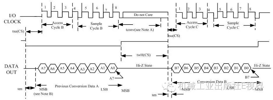 Figure 9 TLC549 Working Timing Diagram
When CS is high, the data output (DATA_OUT) terminal is in a high-impedance state, and at this time, I/O_CLOCK does not take effect. This CS control allows multiple TLC549 chips to be used simultaneously, sharing the I/O_CLOCK to reduce the I/O resource consumption of the MCU when using multiple A-D converters. The process of one conversion operation for TLC549 is as follows:
(1)Set CS low. The internal circuit waits for two rising edges and one falling edge of the internal clock after detecting the falling edge of CS, then confirms this change, and finally automatically outputs the highest bit of the previous conversion result (D7) to the DATA_OUT terminal.
(2)The falling edges of the first four I/O_CLOCK cycles sequentially output the 2nd, 3rd, 4th, and 5th bits (D6, D5, D4, D3), and the on-chip sample-and-hold circuit starts sampling the analog input on the 4th I/O_CLOCK falling edge.
(3)The next three I/O_CLOCK cycles output the 6th, 7th, and 8th conversion bits (D2, D1, D0).
(4)Finally, the on-chip sample-and-hold circuit outputs the 6th, 7th, and 8th conversion bits on the 8th I/O_CLOCK falling edge. The hold function will last for 4 internal clock cycles, and then the A-D conversion will begin for 32 internal clock cycles. After the 8th I/O_CLOCK, CS must be high, or I/O_CLOCK must remain low, and this state must be maintained for 36 internal system clock cycles to wait for the hold and conversion work to complete. If CS is low and a valid interference pulse occurs on I/O_CLOCK, the microprocessor/controller will lose synchronization with the device’s I/O timing; if CS is high and a valid low level occurs, it will reinitialize the pin, thus detaching from the original conversion process.
Before the end of the 36 internal system clock cycles, implementing steps (1)~(4) can restart an A-D conversion, terminating the ongoing conversion, and the output at this time will be the result of the previous conversion, not the ongoing conversion result.
If sampling the analog signal at a specific moment, the falling edge of the 8th I/O_CLOCK clock should correspond to that moment, because the chip starts sampling on the falling edge of the 4th I/O_CLOCK but begins to save on the falling edge of the 8th I/O_CLOCK.
2. Application Subroutine of TLC549
(1)Test Circuit
TLC549 can be easily used with microcontrollers or microprocessors that have a Serial Peripheral Interface (SPI), and can also be connected to the MCS-51 series general-purpose microcontrollers. To verify the reliability of the TLC549 driver program, it can be connected to the ADC0832 application circuit display part, and the interface between TLC549 and MCS-51 series microcontrollers is shown in Figure 10. In this figure, the CS, DATA_OUT (SDO), and I/O_CLOCK of TLC549 are connected to the P3.4, P3.5, and P3.7 interfaces of the microcontroller, respectively. The analog voltage is generated by a potentiometer OP1, and when adjusting the position of the center tap of the potentiometer, the analog voltage changes in the range of 0~5V. The 8-bit data converted by TLC549 is transmitted to the microcontroller serially, and the data range displayed by the microcontroller is 0~255. To achieve a voltage digital detection purpose, this example uses a digital tube to display the voltage value, and the detection result is obtained through program calculation.
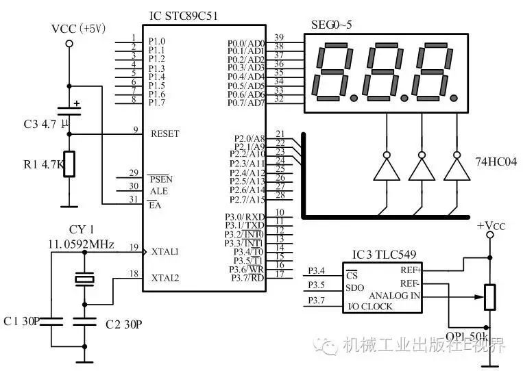 Figure 10 TLC549 Interface Circuit with AT89C51 Microcontroller
(2)TLC549 Subroutine
The TLC549 program is designed according to the timing and operation process of TLC549, including the device initialization function and data conversion function. The specific program is as follows:
/*Preprocessing*/
#include <reg51.h>
#define uchar unsigned char
sbit sd = P3^5; //Data Line
sbit cs = P3^4; //Chip Select
sbit scl = P3^7; //I/OClock
/*Initialize TLC549*/
void tlc549_init(void)
{
cs= 1; //Initialize, Start
scl = 0;
cs = 0;
}
/*Data Conversion for TLC549*/
uchar tlc549_ad(void) //TLC549Processing
{
uchar i,dat_temp = 0;
tlc549_init();
for(i = 0;i < 8;i++) //Read the collected data, reading the last collected data
{
scl= 1;
dat_temp= dat_temp << 1;
if(sd)dat_temp|= 0x01;
scl= 0;
}
cs = 1;
return(dat_temp);
}
(3)Main Program
/*Preprocessing*/
#include<reg51.h>
#include”TLC549.c”
#define uchar unsigned char
#define uint unsigned int
code uchar seven_seg[] ={0xc0,0xf9,0xa4,0xb0,0x99,0x92,0x82,0xf8,0x80,0x90};
uchar cp1,cp2;
uint dat_ad;
/*T0Initialization*/
void timer0_isr(void) interrupt 1 //timer0Interrupt Service Function
{
TL0= (65536 – 5000) % 256;
TH0= (65536 – 5000) / 256;
cp1++;
if(cp1>= 100) //0.5seconds
{
cp1= 0;
dat_ad= tlc549_ad();
dat_ad= dat_ad * 1.96;//Data255Corresponds to Analog Voltage5V
}
P0= 0xff;//Used for simulation to hide
switch(cp2)
{
case0: P0 = seven_seg[dat_ad % 10];P2 = 0x01; break;
case1: P0 = seven_seg[dat_ad / 10 %10];P2 = 0x02; break;
case2: P0 = seven_seg[dat_ad / 100]&0x7f;P2= 0x04; break;//Add Decimal Point
}
cp2++;
if(cp2>= 3)
cp2= 0;
}
/*T0Interrupt Service Function*/
void timer0_init (void) //timer0Interrupt Initialization Function
{
TMOD= 0x01;
TL0= (65536 – 5000)%256;
TH0= (65536 – 5000)/256;
ET0= 1;
EA= 1;
TR0= 1;
}
/*Main Function*/
void main(void) //Main Program
{
timer0_init();
tlc549_init();
while(1);
}
Since TLC549 has only one A-D converter, the program is simpler than that of DAC8032. Both types of A-D converter chips have serial interfaces, reducing the number of connections between the device and the MCU while occupying fewer MCU I/O resources. The downside is that they are slower than similar parallel A-D converters. The timing of A-D converters is relatively simple, so there is greater flexibility in program design.
04classApplication of D-A Converter TLC56151. Working Timing of TLC5615
The working timing of TLC5615 is shown in Figure 11. From the figure, it can be seen that only when the chip select terminal CS is low can serial input data be shifted into the 16-bit TLC5615 shift register. Each rising edge of the SCLK clock will shift one bit of data from DIN into the shift register. Note that the highest bit of data is sent first. After sending 10 bits of data, the rising edge of CS will latch the 10 bits of valid data from the 16-bit shift register into the 10-bit DAC register for the DAC circuit to perform conversion. When the chip select terminal CS is high, data transmission is prohibited. Note that both the rising and falling edges of CS must occur during the low level of SCLK.
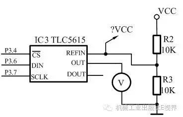 Figure 11 TLC5615 Working Timing
TLC5615 has two working modes. The first mode is single-chip mode, where the 16-bit shift register is divided into 4 high bits as virtual bits, 2 low bits as padding bits, and 10 valid bits. In single-chip mode, only the 10 valid data bits and 2 low padding bits need to be sent to the 16-bit shift register in sequence, and the 2 padding bits can be arbitrary. In single-chip applications, sending data requires 12 SCLK pulses.
The second mode is cascade mode, where the DOUT of one TLC5615 is connected to the DIN of the next TLC5615, requiring the sequence of 16 bits to input the high 4 bits as virtual bits, 10 valid bits, and 2 low padding bits. Because of the addition of the high 4 bits as virtual bits, 16 SCLK pulses are needed.
2. Application Program
(1)Simulation Test Circuit
Figure 12 shows the connection circuit of TLC5615 with the microcontroller. By editing the Proteus simulation circuit, the application program of TLC5615 can be verified. In Figure 12, the /CS, DIN, and SCLK of TLC5615 are connected to the P3.4, P3.6, and P3.7 interfaces of the microcontroller, respectively. The analog voltage output by TLC5615 can be tested with a voltmeter. The reference voltage REFIN is connected to half of the power supply voltage of 5V. When TLC5615 receives all 10 bits of data as 1, theoretically, the OUT terminal will output the power supply voltage of 5V. However, in practical applications, the maximum output will be 4.7V. That is, when the input data of TLC5615 exceeds 961, the output voltage will no longer increase. Therefore, when designing the TLC5615 application program, it is necessary to adjust the input data range.
Figure 12 TLC5615 Connection Circuit with Microcontroller
(2)Application Program
The following application program for TLC5615 is designed to complete a data conversion that changes over time, while the data is displayed on the digital tube. The specific program is as follows:
/*Preprocessing*/
#include<reg51.h>
#include<intrins.h>
#define uchar unsigned char
#define uint unsigned int
const uchar seven_seg[]={0xC0,0xF9,0xA4,0xB0,0x99,0x92,0x82,0xF8,0x80,0x90};
uchar j;
uint moni,dat,i;
sbit din = P1^5;
sbit scl = P1^1;
sbit cs = P1^6;
tlc5615_init(void)
{
cs = 1;
scl = 0;
cs = 0;
}
/* TLC5615Conversion Function*/
void tlc5615(uint dat) //Since TLC5615is ten-bit conversion, define a16bit variable
{
uchar i;
dat <<= 6; //Two bytes have sixteen bits, removing the top six bits leaves ten valid bits
tlc5615_init();//Initialization
for(i = 0;i < 12;i ++)Only ten bits of data need to be sent, but two more zeros need to be added to send a data out
{
din = (bit)(dat& 0x8000);
scl = 1; //The previous sentence can also be replaced withDA= CYbut the order of the latter must be switched
dat <<= 1;
scl = 0;
}
cs = 1;
scl = 0;
}
/* T0Initialization Function*/
void timer0_init(void)
{
TMOD = 0x01;
TL0 = (65536-2000) % 256;
TH0 = (65536-2000) / 256;
TR0 = 1;
ET0 = 1;
EA = 1;
}
/* T0Interrupt Service Function*/
void timer0_isr() interrupt 1 //T0Interrupt Processing Function, Used to Display Output Voltage Value
{
TL0 = (65536-2000) % 256;
TH0 = (65536-2000) / 256;
i++;
if(i >= 500)//0.5seconds
{
i = 0;
tlc5615(dat);
if(dat >= 962)
dat = 0;
moni = dat * 0.489;
dat = dat + 10;
}
P0 = 0xff;
switch(j)
{
case 0 : P0 =seven_seg[moni %10];P2 = 0xfe;break;
case 1 : P0 =seven_seg[moni / 10 % 10];P2 = 0xfd;break;
case 2 : P0 =seven_seg[moni / 100] & 0x7f;P2= 0xfb;break;
}
j++;
if(j >= 3)
j = 0;
}
/* Main Function*/
void main()
{
timer0_init();
while(1);
}
There are many types of A-D and D-A converters, and due to high accuracy requirements, the price of such devices has long remained high. To improve cost-effectiveness, some microcontroller chips integrate A-D and D-A converters internally, such as the STC microcontroller, which integrates an 8-channel A-D converter, thereby increasing the cost-effectiveness of the device. In the applications of A-D and D-A converters, since most of them do not involve chip instructions, program design only needs to send or receive data according to the timing, especially the program design for parallel interface A-D and D-A devices is simpler, which brings great convenience to digital system design.
The external devices used in microcontroller systems are diverse. In the design of microcontroller projects or product development, only by mastering the characteristics of these devices can one design application systems that are functionally perfect and cost-effective.
(-END-)
Excerpted from“Microcontroller Development from Beginner to Proficient” edited by Bai Linfeng et al.
 Special Attention: Reply “1217” in the public account to get the download link

Previous Highlights
Classic Microcontroller Introduction! 25 Project Materials Free Release!
Manufacturing of High-Frequency Transformers
Operating Principles, Circuit Debugging and Testing, Waveform Analysis of Isolated Circuit Controlled by Single Chip Integrated Circuit
PCB Layer Design
PCB Grounding Design