Case Study
Share
Optical Detector of SEM for Z-axis Height Measurement Above Semiconductor Wafer
No.1
01
Problem to be Solved in This Case
1
A semiconductor OEM (Original Equipment Manufacturer) manufacturer wants to add a new feature to their existing SEM (Scanning Electron Microscope) system to enhance productivity. They need a fast and reliable method to position the microscope at the appropriate focal distance above the silicon wafer to identify defects during the production process. The tool is in continuous operation, so they need to perform this as quickly as possible to maximize profits.
02
Solution Provided by Lion Precision
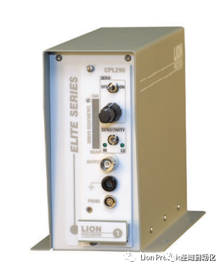
1
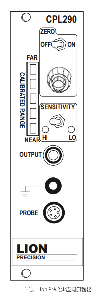
CPL290 Driver + Vacuum-Compatible Capacitive Probe
03
Our Technical Advantages
1
Lion Precision has considerable industry experience in using non-contact capacitive displacement systems for precise measurements. Our high bandwidth, nanometer-level resolution, and vacuum compatibility along with high reliability and custom design capabilities make Lion Precision capacitive sensor systems the best choice for this measurement. This solution allows the optical detector of the electron microscope to quickly move into the focal range above the wafer, with the CPL290 featuring dual ranges and high resolution, optimized to switch on/off within 1ms. The vacuum-compatible capacitive probe with a 45° angle perfectly fits the available space, saving approximately 6 seconds for each operational cycle when customers use Lion capacitive sensors to quickly focus the scanning electron microscope on the wafer.
04
Principle
1
The probe is encapsulated in PEEK (a type of plastic insulation material) to enhance reliability and prevent charging issues in the vacuum chamber. The dual-range options on the CPL290 driver allow the microscope to be positioned at two different heights. The capacitive probe is mounted on the side of the optical system of the electron microscope, and as the microscope moves downwards in the Z direction, the sensor quickly moves it into the focal range above the wafer, allowing the final (fine) focus of the electron microscope to be obtained.
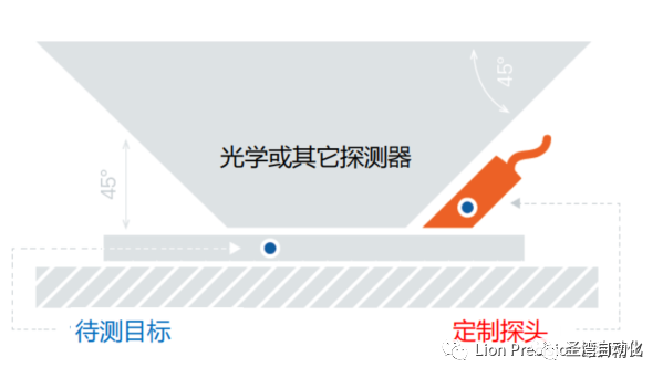
05
Advantages of the 45° Probe
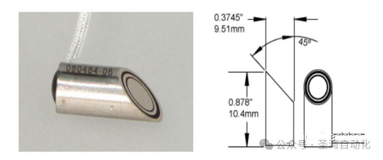
1
As shown in the figure below, this product meets both the space constraints required by the probe and the vacuum compatibility. It is fixed to the side of the electron microscope, and in this structure, the surface of the probe and the surface of the wafer are parallel, ensuring optimal sensor performance in the SEM control system.
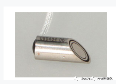
Lion Precision has developed a custom capacitive probe with a 45° surface to fit the available space
06
Significance
1
In this case, with the solution provided by Lion, each operational cycle for the user saves approximately 6 seconds. Since these platforms operate 24/7, this saves a considerable amount of time, allowing customers to inspect more wafers per hour and generate higher revenue. In addition to scanning electron microscopes, our sensors can also be used for Z-direction displacement measurements on other types of microscopes and optical metrology systems, making this case a good reference for customers with unique high-precision applications.
No.2

CPL290 LION PRECISION
No.3
Q: What is SEM??
A: SEM stands for Scanning Electron Microscope, which is a type of microscope that produces images of a sample surface by focusing a beam of electrons on it. The electron beam interacts with the atoms in the sample, generating signals that contain various information about the sample’s surface morphology and composition. The electron beam scans in a raster pattern (a grid of many equally spaced parallel slits) and combines the position of the electron beam with the detection signals to produce images. SEM can achieve resolutions better than 1nm, and samples can be observed under high vacuum conditions using variable pressure SEM, as well as under a wide range of low or high-temperature conditions using specialized instruments.
☁️
Contact for Beijing Saint Bay Automation: Fiona
Phone📞: 15701557738 (same as WeChat)
Email📫: [email protected]