Hello everyone, I am Yi. Let’s continue with the design and selection of current detection circuits.
In the previous article, we analyzed the resistance method for measuring current, and found that the limitation of the resistance method is that it introduces power loss, making it unsuitable for measuring large currents.
For measuring large currents, Hall current sensors are generally used. Hall sensors can measure DC, AC, and complex current waveforms, with a wide measurement range (from tens to thousands of A), and they inherently provide good electrical isolation, high accuracy and linearity, low temperature drift, wide bandwidth, and fast response time. However, they are relatively expensive and cannot be used in environments with strong magnetic field interference.
High-power Hall sensors are shown below, which are larger in size and can measure currents from hundreds to thousands of A.
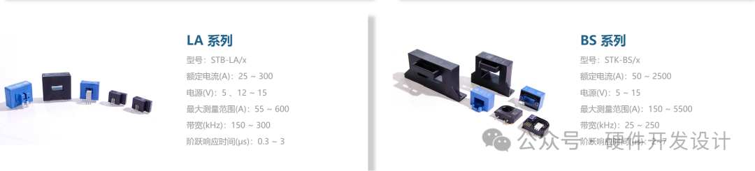
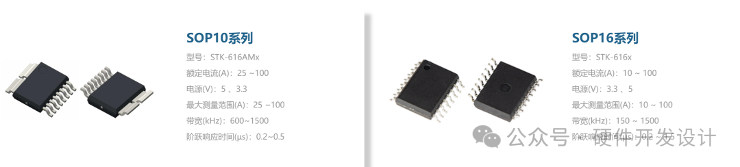
There are also chip-level Hall sensors designed for small current measurements, capable of measuring currents below 100 A.
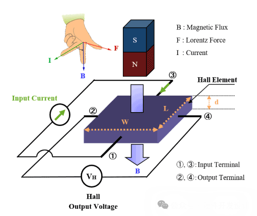
Before using Hall sensors, let’s first understand Hall elements.
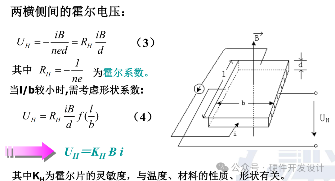
The Hall element is made using the Hall Effect, and it is spelled Hall in English. The name Hall comes from Dr. Hall, who discovered the Hall Effect. The Hall Effect refers to the phenomenon where a potential difference is generated perpendicular to the direction of current flow when a magnetic field perpendicular to the current is applied.
When current flows through a semiconductor film, a voltage is generated that corresponds to the magnetic flux density and its direction based on the Hall Effect.This component, made based on the Hall Effect, which detects the magnetic field is called a Hall element, as shown in the figure below.
The Hall voltage can be expressed with the formula, UH=KH*B*I. Here, B is the magnetic induction strength, and I is the current flowing through the conductor. KH is the sensitivity coefficient.
Hall elements are usually categorized by their output signal type into switching Hall and linear Hall. Switching Hall elements only output two levels of signals, either on or off, which is a digital signal. In contrast, linear Hall elements output a continuously varying analog signal, such as output voltage changing from high to low or low to high, representing a continuous change in an analog signal. For example, non-contact switches and angle sensors used with magnets are switching Hall sensors, while current sensors are linear Hall sensors.
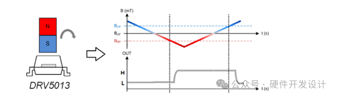
The following figure shows the DRV5013, a Hall sensor with digital latch output switching Hall sensor. It can be seen that it directly outputs logic high and low levels.
The next figure shows the SS39ET Hall sensor chip, which is a linear Hall sensor for detecting magnetic field strength. It can be seen that its output is an analog voltage, which has a linear relationship with the magnetic field.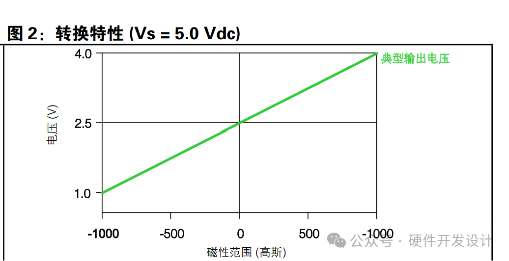
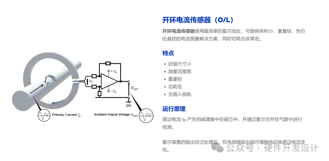
Returning to Hall current sensors, Hall current sensors can be divided into open-loop open-loop current sensors (O/L) and closed-loop voltage sensors (C/L).
Open-loop sensors operate on the principle of Hall direct amplification, and the output of open-loop Hall current sensors is proportional to the magnetic induction strength perpendicular to the Hall chip. The magnetic induction strength is related not only to the measured current but also to the magnetic permeability of the core. The magnetic permeability of the core varies with different currents.
Therefore, open-loop Hall current sensors have poor linearity, lower accuracy, moderate bandwidth, and response time, and larger temperature drift. They are suitable for applications where high accuracy is not critical.
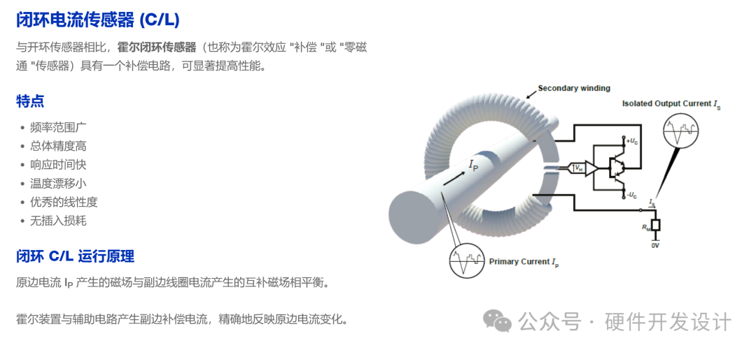
Closed-loop sensors operate on the magnetic balance principle. Closed-loop Hall current sensors consist of primary and secondary windings, where the secondary current is generated by electronic circuits, and the magnetic field generated by this current exactly cancels out the magnetic field generated by the primary current. Thus, the ratio of primary current to secondary current equals the reciprocal of the turns ratio. Because the magnetic fields cancel each other, the actual magnetic flux in the core (as sensed by the Hall chip) is zero, unaffected by the non-linearity of the core, resulting in higher accuracy.
Closed-loop technology also has its limitations, such as significant losses in secondary current (requiring compensation and bias current), larger size (more pronounced in large current sensors), a more expensive structure compared to simpler open-loop designs, and internal voltage drops due to output and secondary winding resistance limiting output voltage. It is suitable for applications requiring high precision, wide bandwidth, and fast response times.
For more details, you can refer to this article.
Principle of Hall Sensors
Hu Yaofan, public account: New Energy BMS Closed-loop Hall Solutions and Magnetic Gate Solutions—Current Sensors
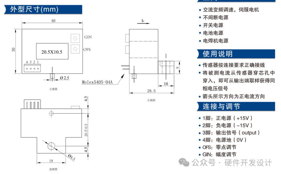
Now, let’s look at a specification sheet for a Hall current sensor.
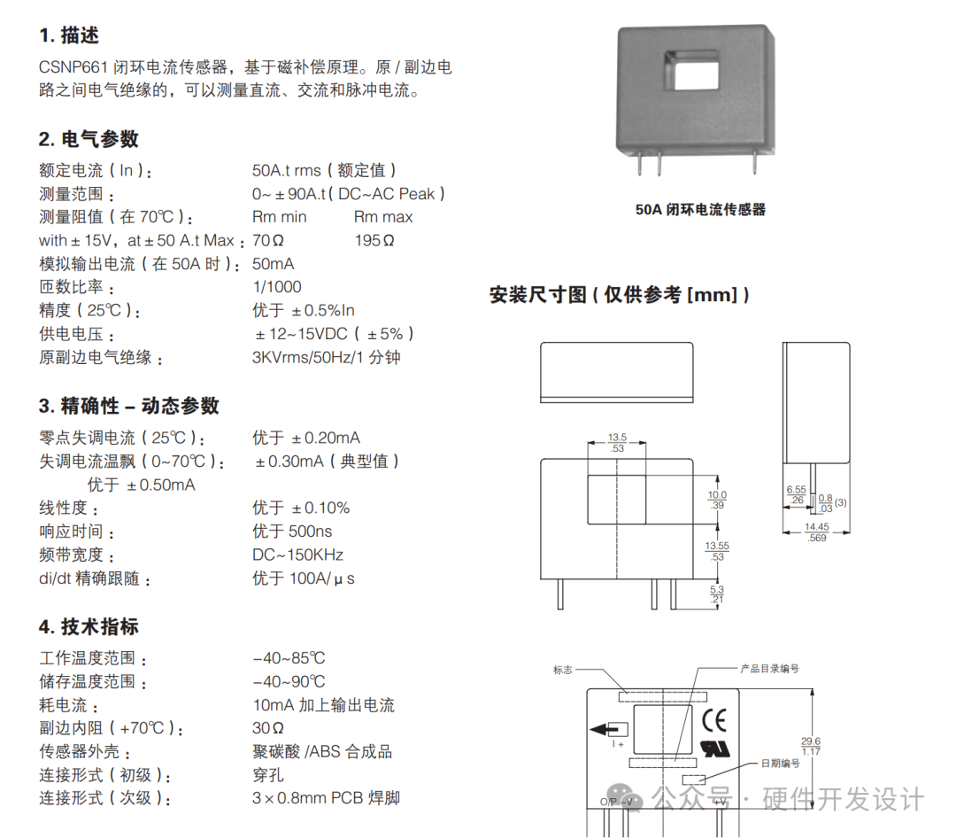
Rated Voltage and Current, referred to as “continuous or rated” current (voltage), indicates the current (voltage) that the sensor can withstand for a long time. Another definition is: the maximum effective value of current (voltage) flowing through the sensor under specified conditions, while ensuring that the temperature under continuous operating conditions does not exceed the limit. This can be tested using a standard 50Hz sine wave signal.
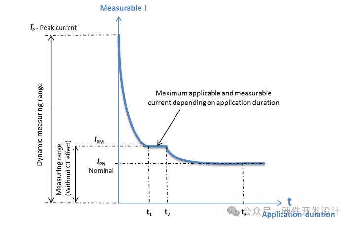
Measurement Range, limited by the maximum measurable peak value under non-steady state. As long as the duration of the current is very short and non-repetitive, the sensor can measure higher current values. This is known as the dynamic measurement range, which is limited by the peak current. In this case, the sensor operates in transformer (CT effect) mode. The maximum peak current will depend on the load (measured) resistance, bus temperature, and sensor structure. Dynamic range and allowable duration (t1…t3).
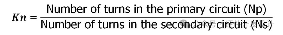
Rated Transformation Ratio K is the ratio of the rated voltage or current on the primary side to the rated voltage or current output. For closed-loop sensors, the transformation ratio NP/NS is approximately the reciprocal of the turns ratio Kr, for example, a transformation ratio of 1:1000 corresponds to the number of turns in the secondary coil (KR = 1000), and when the primary current is 1A, the secondary output current will be 1mA.
 Measurement Resistance or Load Resistance (RM/RB),current output type voltage sensors and current sensors require a load resistance (RB or RM, also referred to as measurement or load resistance) connected to their output to achieve accurate measurement. Closed-loop sensors have an integrated current generator to provide the output signal, while the load resistance is to determine the required optimal current/voltage ratio. The load resistance can convert current into voltage signals, but the value of the resistance must be limited. The measurement resistance must be within a specified range for the sensor to operate safely and effectively.
-
The minimum resistance setting is for thermal protection of the sensor’s output power. For some sensors, the minimum resistance value can be set to 0Ω (considering the maximum power supply voltage during calculation).
-
The maximum resistance setting determines the allowable output range of current/voltage for the sensor. At this time, the sensor output will not saturate. If the measured resistance value is too high, it will reduce the measurement range of the sensor (considering the minimum power supply voltage during calculation).
For example, when the primary current of the above sensor is 50A, the output current at the measurement end is 50mA, with a power supply of +/-15V, the maximum resistance must not exceed 15/50mA=300 ohms.
Why do sensors use current signals?This is because current signals have good resistance to external disturbances, which is especially important when the distance between the sensor’s output signal end and the signal processor of the control circuit is large.
Loss Current IS, refers to the maximum current output from the power supply, that is, the maximum current loss of the current sensor itself when the primary measured current or voltage is zero, plus the output current corresponding to different measured currents. IS This parameter is only applicable to current output type sensors.
When selecting the power supply for closed-loop sensors, special attention is needed. For current or voltage sensors based on closed-loop principles, the current loss IC can be divided into two parts: one part is the fixed loss internal to the sensor, and the other part is the output loss caused by the measured current or voltage (IS).
Output Loss IS can be calculated as follows:
For current sensors: IS output current = primary peak current × transformation ratio
For voltage sensors: IS output current = (primary peak voltage / primary resistance) × transformation ratio
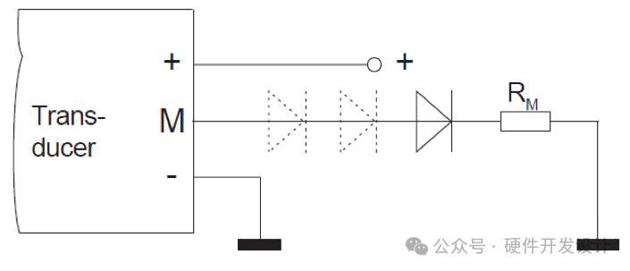
The vast majority of closed-loop sensors require the use of bipolar power supplies (e.g., ±15V). However, if only measuring unidirectional current, many sensors can also operate on a unipolar power supply. In this case, the following points must be considered.
The power supply voltage should equal the sum of the positive and negative voltages indicated in the specification sheet (for example, a sensor of ±15V should use a +30V power supply).
The selection of measurement resistance and maximum operating current should not cause excessive output power consumption by the sensor (please contact LEM for the correct range of measurement resistance values).
The output stage design is for bipolar power supply conditions, and a diode must be connected in series at the output end to achieve minimum output offset voltage, rather than generating a zero-point offset (see the figure below).
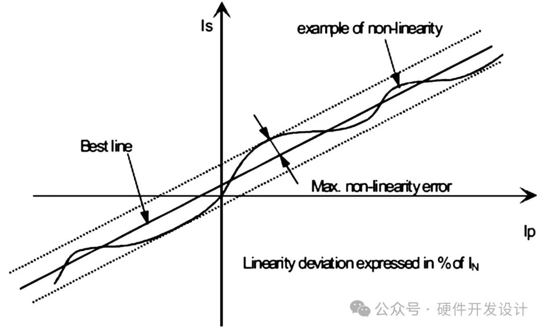
Sensitivity and Linearity
Sensitivity G is defined as the slope of the linear regression line over the entire current range (within the entire ±IPM cycle). Linear error is the difference between the maximum positive or negative measurement point and the linear regression line, expressed as a percentage of the maximum measurement value.
When measuring sensitivity and linearity, the primary DC current cycles from 0 to IPM and then back to 0.
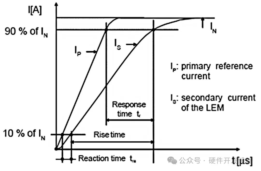
Response Time and Reaction Time
Response time is used to characterize the dynamic characteristics of the sensor. The response time is the time interval from when the primary current reaches 90% of its maximum value to when the sensor output reaches 90% of its maximum value. The slope of the step signal of the primary current is a given value (usually 100A/µs), with an amplitude close to the rated current IPN.
Reaction time Tra is defined as the time interval when both the measured signal and the output signal rise to 10% of the total change.
The above are the basic parameters of Hall current sensors.
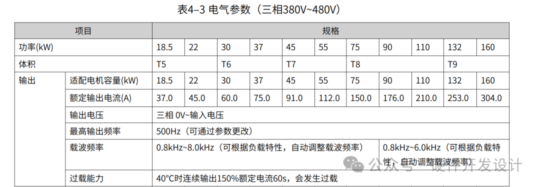
Assume we are making a 132kW inverter, and we find a corresponding specification sheet. We can see that the output parameters of the 132k inverter are as follows:
Rated output current, 253A, 380A at 1.5 times overload;
Carrier frequency, 0.8~8kHz; (i.e., switching frequency, the bandwidth of the current sampling device needs to be much larger than this value, otherwise sampling will be abnormal).
This current is large, making the sampling resistor scheme unsuitable; thus, we can choose an open-loop Hall current sensor.
Since it outputs sinusoidal current, we first determine the peak current, which is a maximum of
The selected Hall linear measurement range must be greater than this value to ensure the accuracy of the measurement signal.
The system carrier frequency of 0.8~8kHz, and considering the response time for system short circuits or overcurrents, we must ensure that the Hall bandwidth is sufficiently large and the response time is sufficiently short.
In summary, a Hall current sensor is selected as follows, which can be seen as a voltage output Hall:
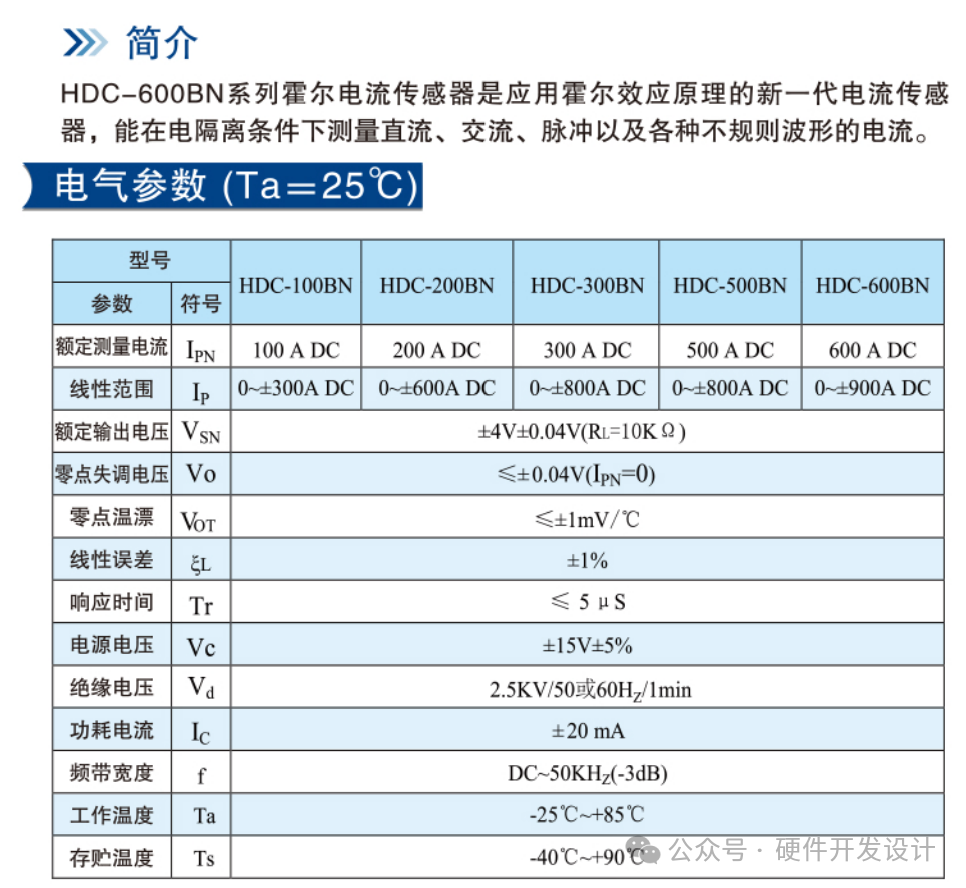
Choose a rated 600A model HDC-600BN.
Its output voltage and input current have an amplification factor of rated voltage/rated current, that is
When using, pay attention to the current direction, which should be consistent with the direction of the sensor arrow, otherwise the phase will be reversed.
The power supply should be as recommended in the specification sheet, using +/-15V.
Next, let’s design a circuit to process the output of the Hall current sensor.
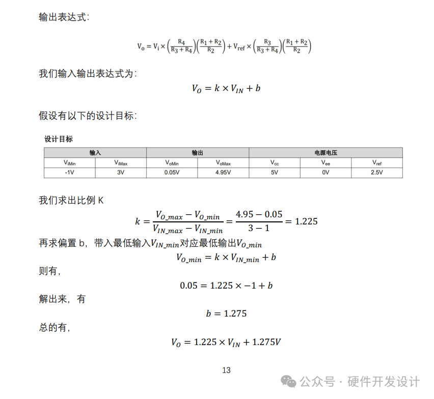
Assuming the ADC reference voltage is 3V, and 2.5 times the rated output current corresponds to the full scale of the ADC, the amplification factor of the subsequent circuit is k, thus:
2.5*253A*1.414*1/150*k+1.5V=3V
Taking the integer value, i.e. 0.25 times. At this time, the full scale is slightly higher than 2.5 times the rated output current.
Note!!!, the output of the Hall current sensor has both positive and negative, while our ADC can only handle positive voltage, so a DC bias must be added to this signal, equal to half of the ADC reference voltage, i.e., 1.5V. This is the reason for the 1.5V in the expression.
Next, we will introduce several circuits that can be used for sensor signal conditioning.
-
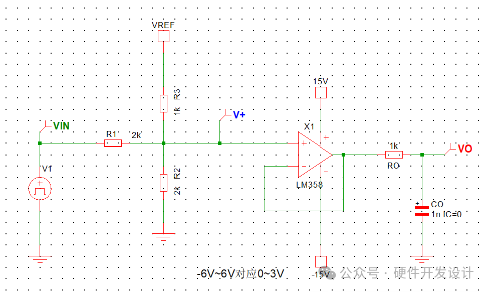
1. Input end with resistor bias (i.e., non-inverting summing amplifier)
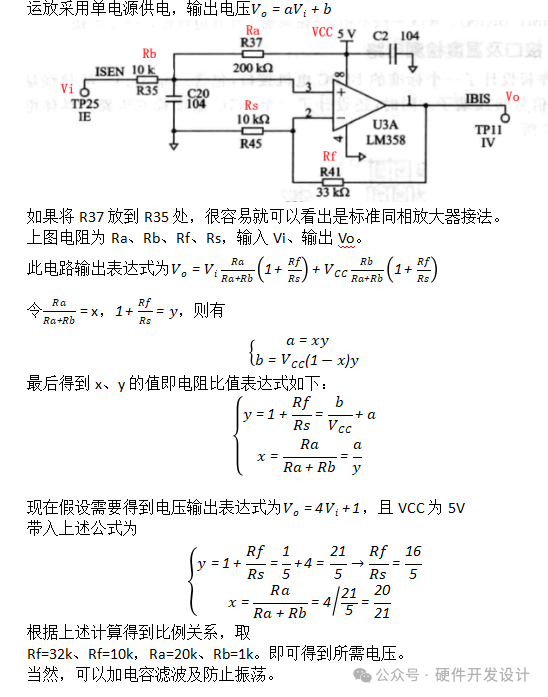
Now, we will calculate the resistance based on the actual parameter values.
VIN linear input range: -900/150V to 900/150V=-6V to 6V.Bias voltage: Take the ADC reference voltage of 3V. Then we can calculate that
We need to obtain the expression: VO=VI*0.25+1.5V,
Substituting into the formula results in
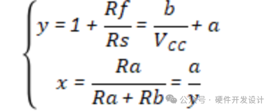
y=1+Rf/Rs=1.5/3+0.25, thus Rf/Rs=-0.25
x=Ra/(Ra+Rb)=0.25/0.75=1/3
Since the resistance calculated is negative, the above circuit is not suitable (this circuit can only be used for amplification).
-
Adding bias to the op-amp input
We will change the circuit by adding another resistor to ground, while the subsequent stage is a buffer output.
For the derivation of resistor bias, refer to the following article:
Traveler Ming Yi, public account: Hardware Development Design How to Use Resistor Bias? This article explains it clearly

We need to obtain the expression:VO=VI*0.25+1.5, substituting gives
x=0.25=1/4,y=1.5/3=0.5, a=1
Substituting into the formula results in
(1/3)=1*(R3/2)/(R1+R3/2),
which simplifies to 1/3=R3/(2*R1+R3)
Choosing R3=2K gives R1=2K, R2=1*2K//2K=1K
The input impedance at this time is R1+R2//R3=2K+2/3K=2.667K
The recommended load resistance in the specification sheet is 10KΩ.

To maintain the ratio, we can simply choose larger resistance values.
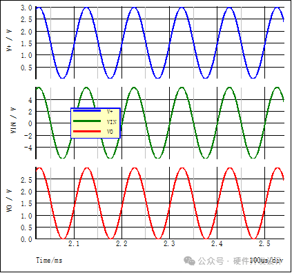
The simulation results are as follows, matching the design values.
-
2. Adding positive bias to the op-amp non-inverting input
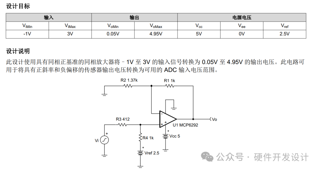
TI derivation is not needed, we will derive it ourselves as follows
VO=VI*0.25+1.5, VREF=3V, R1=R4=R=1K substituted gives
R2=-4K, R3=2K.Resistance calculated as negative, also not applicable.
-
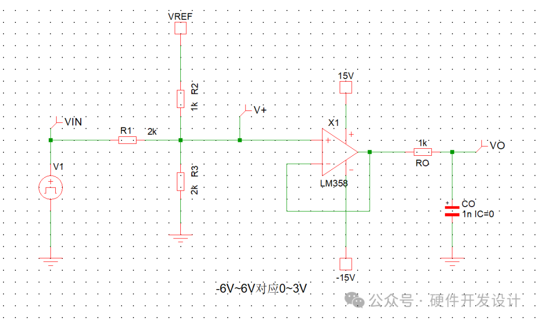
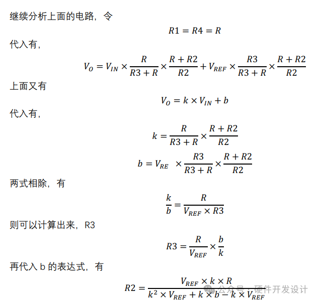
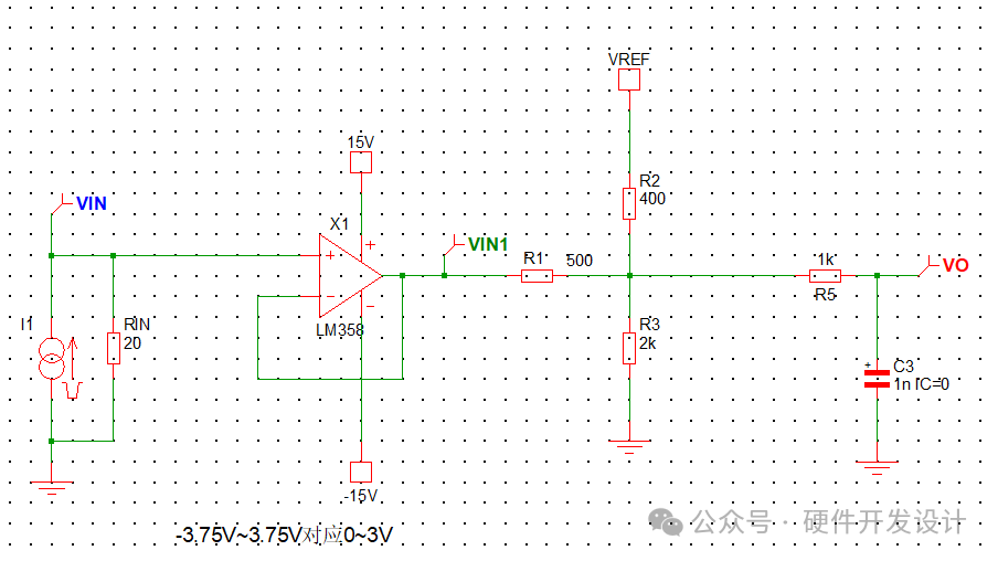
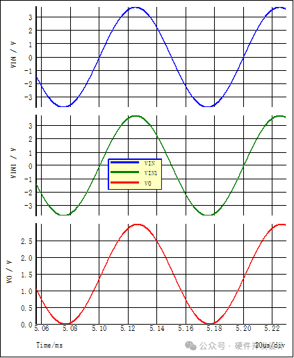
3. Adding bias at the op-amp output
Similarly, see the diagram below. Its principle is the same as that of adding bias at the input.
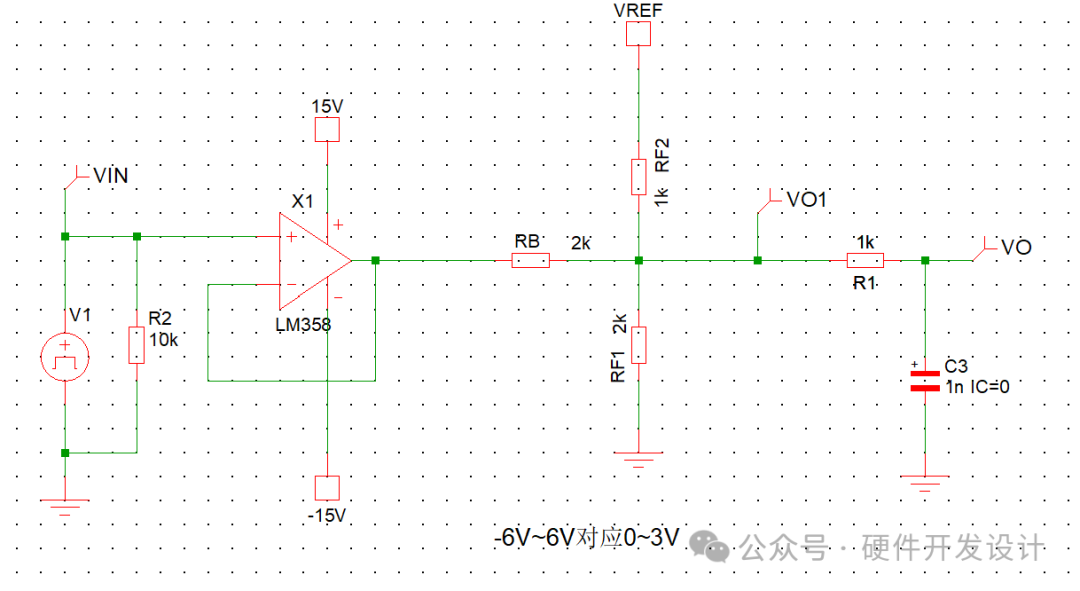
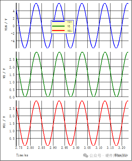
The simulation results are as follows, matching the design values.
The above several circuits are methods for processing voltage output current sensors.
Next, we will introduce the calculation methods for current output Hall sensors, and how to convert voltage to current, refer to the article below.
Methods for Converting Current to Voltage
Traveler Ming Yi, public account: Hardware Development Design to Understand Current to Voltage Signal Circuit Design
Taking the HMC-500LT closed-loop Hall sensor as an example, the specification sheet is as follows:
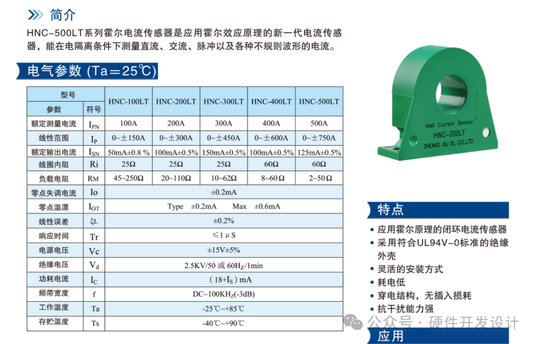
It can be seen that this is a current output Hall sensor, with a current amplification factor of
IS/IP=125mA/500A=0.25mA/A
The recommended load resistance is 2-50Ω, for convenience in calculation, take 20Ω.
Thus, at an input current of 500A, the corresponding output voltage is 125mA*20=2.5V.
At 750A, the output voltage will be 750*0.25*20=3.75V.
Assuming that at 3.75V, the corresponding full scale is 3V, and at –3.75V, it corresponds to 0V.
Thus, the subsequent op-amp output expression is:
VO=VI*3/(3.75–3.75)+1.5=VI*0.4+1.5
Select op-amp output bias circuit to achieve this function.
x=0.4=2/5,y=1.5/3=0.5, a=1
Substituting into the formula results in
(0.4/0.6)=1*(R3/2)/(R1+R3/2),
which simplifies to 2/3=(R3)/(2*R1+R3)
Choosing R3=2K gives R1=1/2K, R2=1*2K//(1/2K)=0.4K
Simulation results are as follows:
Simulation results match the calculations.
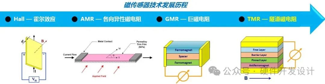
Tunnel magnetoresistance (TMR) devices are the next generation of magnetic sensitive devices after Hall devices, anisotropic magnetoresistance (AMR), and giant magnetoresistance (GMR), characterized by low power consumption, low temperature drift, and high sensitivity. In current sensors, replacing Hall devices with TMR can significantly improve the sensitivity and temperature characteristics of current sensors.
That is, TMR has better characteristics, the following figure is a diagram of the upgrade of four generations of magnetic sensing technology.
Based on TMR, closed-loop current sensors generally have four pins: Power Supply +, Power Supply –, Reference Output Vref, Output Vout.
The output voltage Vout fluctuates around the reference voltage Vref as the zero point.
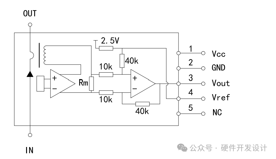
Using the STB-250LA/Z as an example, let’s study the specification sheet.
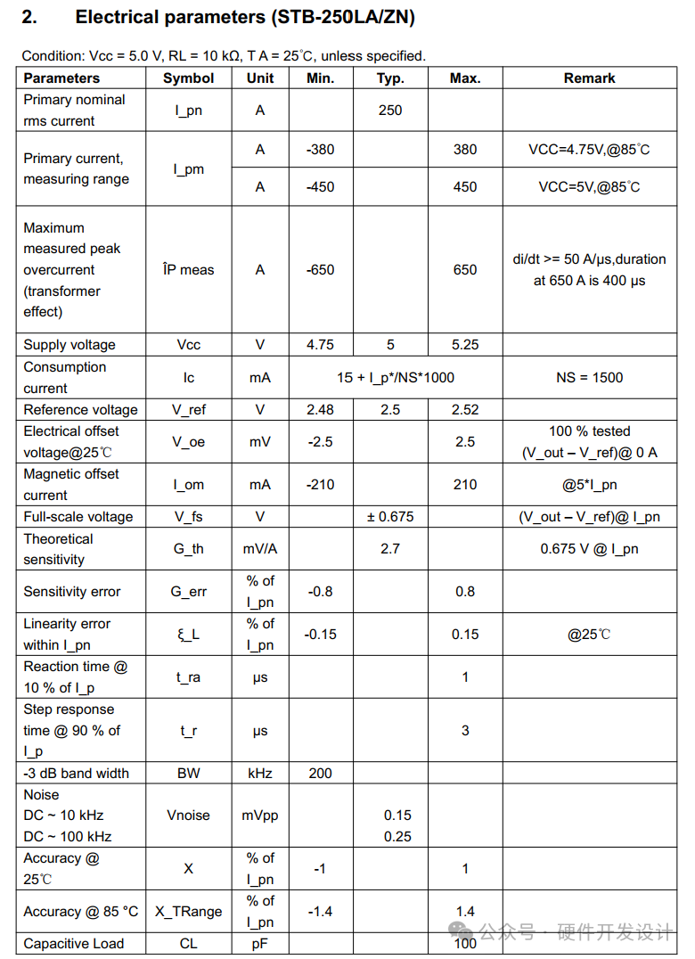
It can be seen that it can be powered easily with a 5V single power supply.
The amplification factor of the output voltage to the input current is G_th=2.7mV/A.
Using a differential amplifier, this signal can be processed and sent to the ADC. The circuit diagram is as follows:
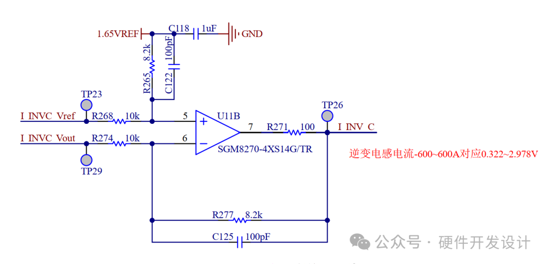
This is a basic differential amplification circuit. Regarding the calculations for differential amplification with bias, the previous articles have detailed it, so we will not elaborate further. Please refer to this article.
Single Power Supply Differential Detection Circuit
Traveler Ming Yi, public account: Hardware Development Design High Resistance with Differential Detection Supplement
The above is the application of large current sensors, while the design and selection of small current detection ICs below 100A will be explained in future articles.
Reply with the keyword: “Current Detection Data 2” to obtain the data
-
Hall Effect – Current Sensor Technology——LEM
-
TMR Magnetic Sensor Overview——Multidimensional Technology
-
https://static.sensorexpert.com.cn/upload/file/20200424/1587713400851165.pdf——Honeywell
-
https://www.ti.com/cn/lit/an/zhca763a/zhca763a.pdf?ts=1690396996741——TI
—————————————————
In Conclusion
That’s all for this introduction, thank you all.
If there are any errors in this article, everyone is welcome to criticize and correct.
If you find my article helpful, please like and share it. Thank you!
—————————————————