
The MIPI (Mobile Industry Processor Interface) interface, especially its physical layers D-PHY and C-PHY, is widely used in high-speed data transmission scenarios such as cameras (CSI-2) and displays (DSI-2). The PCB layout and routing of MIPI are crucial for signal integrity, directly affecting the performance and reliability of devices. Below are key guidelines for MIPI interface PCB layout and routing:
Core Principles: Control impedance, minimize crosstalk, ensure equal length, provide complete return paths, and reduce losses.
1. Key Design Requirements
Differential Impedance Control:
MIPI D-PHY uses differential signals (Clock+/- and DataN+/-). The differential impedance must be strictly controlled at 100Ω ±10%.
Implementation:
Precise Layer Stack Design: Work closely with PCB manufacturers to determine the exact board materials (such as FR4, preferably Low-Dk/Df materials like Megtron 6/7, Isola 370HR, etc.), layer thicknesses (especially the dielectric thickness between signal layers and reference planes), and copper thickness.
Calculate Trace Width and Spacing: Use impedance calculation tools (such as Polar SI9000, Ansys SIwave, Cadence Allegro PCB SI, etc.) to calculate the required trace width and trace spacing to achieve 100Ω differential impedance based on the selected stack parameters.
Consistency: The width and spacing of the traces in the entire differential pair must remain constant. Avoid sudden changes near connectors, vias, and component pads.
Single-ended Impedance Control (C-PHY and D-PHY Clock):
MIPI C-PHY uses three single-ended signals.
The clock line of D-PHY is also a differential pair.
These single-ended signals or single traces in the differential pair typically require single-ended impedance to be controlled at 50Ω. Precise layer stack and trace width design are also required to ensure this.
2. Layout Strategies
Component Placement:
Close to Connectors: Place the MIPI transmitter (such as the application processor) and receiver (such as camera modules and displays) as close as possible to minimize trace length. Short traces mean lower losses and fewer opportunities for interference.
Avoid High-Speed Digital Interference Sources: Keep away from noise sources such as CPUs, DDR memory, switch-mode power supplies, crystal oscillators, and RF modules. Maintain sufficient spacing (at least 3-5 times the trace width or as determined by simulation).
Same Layer Routing Priority: Ideally, the entire MIPI differential pair or single-ended group should be routed on the same signal layer, avoiding unnecessary vias. If layer changes are necessary, strictly control the number of vias and optimize the design.
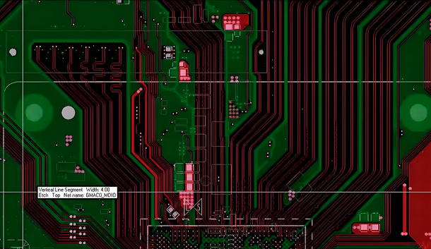
Stack Structure:
Prefer Stripline Structure: Route MIPI traces in inner layers (such as L2 or L3), sandwiched between two complete, uninterrupted ground planes (GND). This provides the best shielding and impedance control environment.
Avoid Microstrip (Outer Layer) Routing: If routing must be done on the outer layer, care must be taken to ensure a complete reference plane and enhance shielding measures (such as dense ground copper and ground vias), but performance is generally not as good as inner layer stripline.
Complete Reference Plane: The reference layer below the MIPI traces must be a continuous, complete ground plane. Absolutely avoid crossing power plane splits or routing other signal lines beneath the MIPI traces. Discontinuities in the reference plane can severely disrupt impedance and return paths.
Recommended Stack Example (4-layer board):
Top Layer (L1): Components, low-speed signals, power
GND Plane (L2): Complete ground plane
Signal Layer (L3): High-speed signals (MIPI traces)
Bottom Layer (L4): GND Plane / Power Plane (if serving as the reference plane for L3, it must be complete)
Recommended Stack Example (6-layer board or more): More flexibility, typically routing high-speed signals on L3/L4, with GND planes above and below.
3. Routing Rules
Differential Pair Routing:
Equal Length Matching: The lengths of the P and N traces within the differential pair must be strictly equal. Length differences are typically controlled to < 5 mils (0.127mm) and a maximum of 10 mils. Use the equal length routing function in PCB design software.
Close Coupling: The P and N traces should maintain a calculated constant spacing throughout their path. Avoid unnecessary widening of the spacing.
Symmetry: The P and N traces should be as symmetrical as possible (consistent trace width and spacing from surrounding objects).
Minimize Bends: Avoid 90° right-angle bends, using 45° angles or arcs. The spacing at bends should remain consistent.
Avoid Splitting: The two lines of the differential pair should be treated as a whole, avoiding being forcibly separated by vias, pads, or other traces. If separation is necessary (e.g., to bypass obstacles), the distance apart should be as short as possible, and they should be re-coupled as soon as possible.
Intra-Pair Channel Matching (for multi-channel CSI/DSI):
The lengths of different data channels within the same group (e.g., Data0, Data1, Data2, Data3 for CSI-2) and their lengths relative to the clock channel also need to be matched.
Matching tolerances are usually more relaxed than those within the differential pair, but it is recommended to control within < 50 mils (1.27mm), with stricter design requirements within 25 mils. Specific requirements should refer to device manuals and timing budgets.
Clock pairs are typically used as a reference, with other data channels matched to them.
Via Design:
Minimize Vias: The number of vias on each differential pair or critical single-ended signal should be absolutely minimized (ideally 0, at most 1-2). Each via is a point of impedance discontinuity and a potential source of reflection.
Symmetrical Via Placement: If a differential pair must use vias, the P and N vias should be placed in pairs and closely adjacent, maintaining symmetry.
Optimize Via Structure: Use the smallest possible drill diameter and pad diameter. Consider using back drilling to remove unused via stubs. In high-speed designs, microvias or laser drilling may be required.
Ground Via Accompaniment: Place 1-2 ground vias near each signal via (< 20 mils) to provide the shortest return path for the signal.
Spacing Rules:
Differential Pair Spacing: Sufficient spacing between different differential pairs (e.g., CLK and Data0, Data0 and Data1) should be maintained to reduce crosstalk. The minimum recommended spacing is 3 times the differential trace width or the 3W rule (W is the trace width). The larger, the better, if space allows. For example, if the trace width is 5 mils, the spacing of 5 mils (differential spacing) means that the spacing between different pairs should be at least 3*(5+5) = 30 mils.
Spacing with Other Signals: MIPI signals must maintain a spacing much greater than 3W from any other signals on the board (especially other high-speed signals like DDR, USB, LVDS, etc.). Recommended 10W or more, with ground copper isolation in between.
Spacing with Board Edge: Maintain sufficient distance between MIPI traces and the PCB edge (at least 50 mils) to avoid radiation and external interference.
Shielding and Grounding:
Ground Copper Treatment: Lay continuous ground copper on both sides and above the MIPI differential pair or signal group (if on the outer layer). This is not the main return path (the reference plane is), but it provides additional shielding.
Dense Ground Via Array: Along the path of the MIPI traces, place a row or multiple rows of ground vias with tight spacing (e.g., 100-200 mils spacing) to closely connect the top/bottom ground copper with the internal ground plane, forming a “Faraday cage” effect to effectively suppress radiation and external interference. This is a critical measure!
Connector Shielding: The metal shell of the MIPI connector must be connected to the main ground plane of the PCB through multiple low-impedance paths (multiple vias, wide copper).
Power Integrity:
Provide clean and stable power to the MIPI transmitters and receivers. Use appropriate decoupling capacitors (typically a combination of 0.1uF and 1-10uF) and place them close to the power pins of the devices.
Power plane splits should be reasonable to avoid noise coupling onto the power for the MIPI circuits.
4. Other Important Considerations
ESD Protection Devices:
If ESD protection devices (such as TVS diodes) are used, they must be placed extremely close to the connector (before the MIPI signal lines enter the connector). Traces after the protection devices should also be routed according to high-speed rules.
The ground end of the protection device must be connected to the connector shield ground or main ground plane via the shortest path (wide traces, multiple vias).
Test Points:
Reserve small test points (such as surface mount pads) on key signals (CLK±, DataN±) for debugging and testing. Test points must be very small and should not disrupt the symmetry and impedance of the differential pair. Ideally, they should be designed on reserved branches rather than directly in series on the main path. Avoid opening the reference plane below the test points.
Series Resistors:
Sometimes a small resistor (such as 10-100Ω) is placed in series with the differential output at the transmitter for impedance matching and reducing reflections. This resistor must be placed very close to the transmitter chip.
Simulation Verification:
Strongly recommended to perform signal integrity simulation: Use tools like HyperLynx, ADS, SIwave, etc., to simulate before PCB fabrication, checking for impedance continuity, insertion loss, return loss, crosstalk, eye diagram quality, and other metrics to ensure compliance with specifications. Simulation can identify potential issues early, avoiding costly rework.
Summary Key Points Quick Reference
|
Characteristic |
Requirements/Recommended Values |
Key Measures |
|
Differential Impedance |
100Ω ±10% |
Precise layer stack design, calculate trace width/spacing, maintain consistency |
|
Single-ended Impedance |
50Ω (C-PHY, D-PHY clock single-ended) |
Precise layer stack design, calculate trace width |
|
Stacking |
Prefer inner layers (stripline) |
Route traces sandwiched between two complete GND planes |
|
Reference Plane |
Complete, continuous GND |
Avoid splits, slots, or other signals below |
|
Differential Pair Equal Length |
< 5 mils (0.127mm) |
Use software equal length routing function |
|
Intra-group Channel Equal Length |
< 50 mils (1.27mm) |
Clock pair as reference, data pairs matched to it |
|
Vias |
Minimize (0-2) |
Symmetrical placement, small size, accompany with GND vias, consider back drilling |
|
Differential Pair Spacing |
Constant (according to impedance calculation) |
Avoid unnecessary widening |
|
Different Pair Spacing |
≥ 3W (trace width W) / Recommended ≥10W |
The larger, the better if space allows |
|
Spacing with Other Signals |
Much greater than 3W / Recommended ≥10W |
Use ground copper isolation |
|
Bends |
45° or arcs |
Avoid 90° angles |
|
Ground Vias |
Dense array along traces (100-200 mil spacing) |
Connect top layer ground copper to main GND plane, forming shielding |
|
Grounding |
Lay ground copper on both sides |
Provide additional shielding (not the main return path) |
|
ESD Protection |
Extremely close to the connector |
Short, wide ground connections |
|
Decoupling Capacitors |
Near device power pins |
0.1uF + 1-10uF combination |
|
Simulation |
Strongly recommended |
Verify SI performance before fabrication (impedance, loss, eye diagram) |
Strict adherence to these guidelines, combined with specific device data sheet requirements and SI simulation results, is key to ensuring high-speed, reliable, low-noise transmission of the MIPI interface on PCBs. High-speed design has no “close enough”; details determine success or failure. When designing for the first time, be sure to leave margins and conduct thorough simulation verification. If needed, you can provide your specific design details (such as stack, trace width, spacing, length, etc.), and I can help you analyze further.
Let’s delve into the specific details ofMIPI interface PCB design. These details will translate the previous guidelines into executable parameters and structures. Please note that the final parameters must be based on the PCB materials, stack structure, manufacturing capabilities, and target rates you choose, and confirmed through impedance calculation tools and simulation verification.
Core Premise:
Clarify Specifications: Confirm whether it is D-PHY (mainstream) or C-PHY? What is the target data rate (e.g., 1.5Gbps, 2.5Gbps per lane)? This affects loss budget and equal length requirements.
Select Board Material: Standard FR4 (such as S1141) can be used for lower rates (<1.5Gbps). For high rates (≥2.5Gbps) or long traces (>100mm), it is strongly recommended to use low-loss materials (such as Panasonic Megtron 6/7, Isola FR408HR/TeraGreen 400G, Nelco N4000-13 EPSI, Rogers 4350B – higher cost).
Determine Layer Stack: Work closely with PCB manufacturers to determine the number of layers, thicknesses of each layer (copper thickness and dielectric thickness), order, and materials.

1. Layer Structure & Impedance Calculation Specific Example (Adjust as Needed!)
Assumed Target: D-PHY, Differential Impedance 100Ω, Single-ended 50Ω, using standard FR4 (Er≈4.2 @1GHz).
Example 1: 4-layer Board (Preferred Structure)
|
Layer Order |
Layer Name |
Copper Thickness (oz) |
Usage/Description |
Distance to L2 (mil) |
Distance to Reference Layer (mil) |
|
L1 |
Top (Component Layer) |
1 |
Low-speed signals, power, decoupling capacitors, connectors |
– |
– |
|
L2 |
GND Plane |
1 |
Complete, uninterrupted ground plane! The main reference plane for MIPI traces. |
– |
– |
|
L3 |
Signal |
1 |
High-speed signal layer (MIPI traces) |
H1 = 5.0 mil |
H1 = 5.0 mil |
|
L4 |
Bottom/PWR |
1 |
Power plane or ground plane. If serving as the secondary reference plane for L3, it must be a complete plane! |
H2 = 28.0 mil |
H1 + H2 = 33.0 mil |
MIPI Trace Layer: L3 (Stripline Structure)
Reference Plane: Above L2 (GND), below L4 (GND or PWR – preferably GND). If L4 is PWR, ensure it is a complete, low-noise power plane.
Impedance Calculation (using tools like Polar SI9000):
Model Selection:<span>Broadside-Coupled Stripline</span> (stripline edge-coupled differential pair) or <span>Embedded Microstrip</span> (if L4 is PWR and sufficiently far, primarily referencing L2, then this model is close – needs confirmation).
Key Input Parameters:
<span>H1</span>: Distance from signal layer to upper reference plane (e.g., 5.0 mil)
<span>H2</span>: Distance from signal layer to lower reference plane (e.g., 28.0 mil – If L4 is GND and the primary reference, H2 needs to be symmetrical with H1. In this case, L4 may be PWR, H2 larger, primarily referencing L2).
<span>Er</span>: Dielectric constant (FR4 ≈ 4.2, accurate value @ frequency provided by board material supplier)
<span>T</span>: Trace copper thickness (1 oz = 1.4 mil finished, 0.5 oz = 0.7 mil – commonly use 0.5 oz for fine traces)
<span>Target Zdiff</span>: 100Ω, <span>Target Zse</span>: 50Ω
Calculation Result Example (estimation, needs tool confirmation!):
Differential Pair (100Ω):<span>Trace Width (W) = 4.5 mil</span>, <span>Trace Spacing (S) = 5.5 mil</span>
Single-ended (50Ω):<span>Trace Width (W_se) = 8.5 mil</span> (for C-PHY single line or D-PHY clock single estimation)
Note: L4 is far from L3 (33mil), L3 primarily references L2. L4’s role is to shield against interference below. Ensure L4 plane below L3 traces is uninterrupted in the projection area!
Example 2: 6-layer Board (More Optimal, Higher Flexibility)
|
Layer Order |
Layer Name |
Copper Thickness (oz) |
Usage/Description |
Distance to Reference Layer (mil) |
|
L1 |
Top (Component Layer) |
0.5 / 1 |
Components, low-speed signals |
– |
|
L2 |
GND Plane |
1 |
Complete ground plane |
– |
|
L3 |
Signal |
0.5 |
High-speed signal layer 1 (MIPI traces) |
H1 = 4.5 mil (to L2) |
|
L4 |
Signal |
0.5 |
High-speed signal layer 2 or low-speed |
H2 = 10.0 mil (to L5) |
|
L5 |
PWR Plane |
1 |
Complete power plane (or reasonably split) |
– |
|
L6 |
Bottom |
0.5 / 1 |
Components, low-speed signals |
– |
MIPI Trace Layer: L3 (Stripline Structure)
Reference Plane: Above L2 (GND), below L5 (PWR). Key: L5 must be a complete, low-noise power plane in the area below the MIPI traces! If L5 is split or has high noise, this structure is not as ideal as symmetric stripline.
Alternative (More Optimal): Place high-speed signals on L3 and L4, with L2 and L5 as complete GND. This way, L3 references L2 and L5 (distances H1 and H2), and L4 also references L2 and L5 (distances H2 and H3). This is a more symmetrical and optimal stripline environment.
Impedance Calculation:
Model:<span>Broadside-Coupled Stripline</span> (if both upper and lower reference layers are GND and distances are symmetrical) or <span>Asymmetric Stripline</span> (asymmetrical).
Input: H1 (L3 to L2), H2 (L3 to L5), Er, T.
Calculation Result Example (estimation):
Differential Pair (100Ω):<span>W = 4.0 mil</span>, <span>S = 5.0 mil</span> (0.5oz copper thickness, H1=4.5mil, H2=10mil – asymmetrical).
Target: Design to make the distances to the upper and lower reference layers equal (H1 ≈ H2 ≈ 5-7mil) for optimal symmetry and impedance control.
Key Conclusion:
Inner layer stripline is optimal. The preferred signal layer is sandwiched between two complete GND planes with symmetrical distances.
Copper Thickness: High-speed signal layers commonly use 0.5 oz finished copper thickness, allowing finer trace widths to achieve target impedance.
Dielectric Thickness: The distance from the signal layer to the reference plane (<span>H</span>) is a core parameter for impedance calculation, controlled by the PCB manufacturer through the layer stack. This value is usually small (4-8mil) and needs to be precise.
Impedance Calculation Tools Must Be Used! Request the PCB manufacturer for an accurate layer stack table (including materials, thicknesses, copper thickness, Er values), input the tools to calculate<span>W</span> and<span>S</span>. Require the manufacturer to perform controlled impedance and provide feedback on measured results.
2. Routing Rules Specific Parameters (Based on Typical Scenarios)
Differential Pair Equal Length (Intra-Pair Skew):
Absolute Requirement:< 5 mils (0.127mm). This is a hard requirement.
Design Target:< 2 mils. Use EDA tools’ differential pair routing and equal length routing (Tuning/Matching) functions to achieve.
Serpentine Routing:
Amplitude (Amplitude) ≥ 3 times the trace width (3W). For example, if the trace width is 4mil, amplitude ≥ 12mil.
Use 45° angles for corners. Arcs are also acceptable, but 45° is easier to control spacing and has better processing consistency.
Spacing (spacing between serpentine segments) ≥ 2 times the amplitude or 3W (whichever is larger), to avoid self-crosstalk. For example, if the amplitude is 12mil, spacing ≥ 24mil.
Inter-Pair Channel Matching (Inter-Pair Skew / Inter-Lane Skew):
Target Range:< 25 mils (0.635mm) to < 50 mils (1.27mm). Specifics depend on data rate and protocol requirements (CSI-2/DSI specifications usually have recommended values, check the main control and device Datasheet!). Clock pairs (CLK±) are typically used as a reference.
Design Strategy: First ensure that all differential pairs meet equal length requirements, then match the lengths of all data channels (Data0±, Data1±…) to the clock channel (CLK±) within tolerance ranges. Matching is usually done near the receiving end.
Spacing Rules (based on W = trace width, e.g., W=4-5mil):
Differential Pair Internal Spacing (S): Remain constant! Set according to impedance calculation results (e.g., S=5.0mil). Avoid widening for equal length routing!
Spacing Between Different Differential Pairs (Edge to Edge):
Minimum:3W (e.g., 12-15mil). This is the bottom line.
Recommended:≥ 5W to 10W (e.g., 20-50mil). The larger, the better if space allows, significantly reducing crosstalk. Especially important between CLK and Data pairs!
Implementation: Insert ground tracks (GND Track) between different pairs in parallel routing and fill with dense ground vias (GND Via Stitch). This is a very effective method.
MIPI Signal Spacing with Any Other Signals (Edge to Edge):
Minimum:≥ 20W (e.g., 80-100mil). Strongly recommended ≥ 30W (e.g., 120-150mil).
Implementation: Use wide copper isolation areas, and fill with ground vias. Avoid other high-speed signals (USB, DDR, LVDS) close to the MIPI area.
Spacing with Board Edge:≥ 50 mils (1.27mm). Ideally ≥100mils. Lay ground and add vias at the edges.
Via Design (Critical!):
Number:≤ 2 / differential pair (including layer changes and connectors). Ideally 0. Each via is a point of impedance change.
Type:
Laser Microvias (HIDI/Microvia): Best choice, short or no stubs, small parasitic parameters. Higher cost.
Mechanical Through Hole Vias: Commonly used. Must require back drilling! To remove unnecessary long stubs from unconnected layers.
Size (Typical Mechanical Via):
Drill Diameter: 8 mil (0.2mm). The smaller, the better, limited by board factory capabilities.
Pad Diameter: 18 mil (0.45mm). Meet minimum annular ring requirements.
Anti-Pad: ≥ 34 mil (0.86mm). The isolation ring around the via pad on the reference layer ensures that signals do not short to the reference plane. Sufficiently large anti-pads are crucial for impedance continuity! The anti-pad diameter on the reference plane layer should be at least8-10mil larger than the pad diameter.
Placement:
Symmetrical: The vias of the differential pair must be paired, closely adjacent, and mirror-symmetrical in placement. Maintain symmetry in P/N paths.
Accompanying GND Vias: Place at least 1 (preferably 2) ground vias near each signal via (< 15 mils). These GND vias connect all reference layers, providing the shortest return path. This is key to suppressing impedance changes and radiation!
Back Drilling: Must be required! Specify back drill depth to ensure removal of long stubs from unconnected layers. Stub length should be < 10 mils.
Ground Shielding Structure:
Copper Layer: Lay ground copper on both sides of the MIPI trace layer (L3), with a width of ≥ 20 mils. This is not the main return path (the reference plane is), but provides additional shielding.
Ground Via Array (Via Fencing):
Location: Along both sides of all MIPI traces (differential pairs or C-PHY three-line groups).
Spacing:100 mils (2.54mm) center-to-center. For ≥2.5Gbps or sensitive designs,50 mils (1.27mm) center-to-center. The denser, the better!
Via Type: Standard mechanical vias are sufficient (e.g., Drill=8mil, Pad=16-18mil).
Connection: Connect the ground copper of the top layer (L1/L4) to all internal ground planes (L2/L5) with low-impedance connections.
Connector Shielding: The metal shell of the MIPI connector must be connected to the main ground plane of the PCB through multiple (≥4) low-impedance paths:
Use wide copper (≥100mils) for connection.
Place dense ground vias around the connector pads (spacing ≤100mils).
Ensure that all layers below the connector (especially adjacent signal layers) have large areas of ground and are connected to the main GND.
ESD Protection Device Layout:
Location: Close to the signal pins of the MIPI connector. Trace order:<span>Connector Pin -> ESD Device Signal Pin -> MIPI Main Trace</span>.
Routing: The traces before the ESD device should be as short as possible (<100mils). The transition from the ESD device to the main trace should also be short and symmetrical (for differential pairs).
Grounding: The GND pin of the ESD device should be connected with the shortest, widest trace (≥20-30mil) to the shield ground pad of the connector or nearby main GND plane, and fill with multiple GND vias.
Series Resistors:
Location: Close to the MIPI Tx output pin of the transmitter chip (AP/CP).
Routing: The trace to the chip pin should be extremely short (<50mils). The traces after the resistor should start routing according to 100Ω differential impedance.
Selection: 0402 or smaller package (0201), to reduce parasitic effects.
Test Points:
Type: Prefer small surface mount test pads (e.g., round or square, diameter/side length ≤ 15 mils). Avoid using through-hole test points.
Location: Ideally designed on short branch lines (Stub), rather than directly in series on the main differential path. Branch line length < 50 mils.
Symmetry: Test points of the differential pair must be symmetrically placed.
Reference Layer Below: The reference layer (GND/PWR) directly below the test point must not be opened! Keep it continuous.
3. Design Checklist (Must Confirm Before Fabrication)
Layer Stack: Have you obtained the final, accurate layer stack table from the board factory? (Materials, thicknesses, copper thickness, Er values)
Impedance: Have you calculated W and S using the layer stack table in SI9000 or similar tools? Have the results been provided to the board factory for impedance control? Is the target impedance (100Ω diff, 50Ω se) clearly marked in the Gerber/fabrication requirements?
Trace Layer: Is MIPI routed in inner layers (stripline)? Is the reference plane complete and uninterrupted (especially in the projection area below the traces)?
Equal Length:
Is the length difference within the differential pair < 5 mils? (Tool DRC check)
Are all Data Lane lengths vs Clock Lane lengths within target tolerances (<25/50mils)? (Tool DRC check)
Does the serpentine line meet amplitude ≥3W, spacing ≥2 times the amplitude?
Spacing:
Is the internal spacing of the differential pair constant?
Is the spacing between different differential pairs ≥ 5W? (Especially pay attention to CLK-Data)
Is the spacing between MIPI and other signals ≥ 20-30W? Is there ground copper isolation?
Is the distance from the board edge ≥ 50mils?
Vias:
Is the number ≤ 2 per differential pair? Are they symmetrically placed?
Are the sizes (Drill/Pad/Anti-Pad) optimized? Is the anti-pad sufficiently large?
Is back drilling clearly required?
Is there ≥1 ground via adjacent to each signal via (<15mils)?
Grounding:
Are there ground vias fencing along both sides of the MIPI traces? Is the spacing ≤100mils (recommended 50mils)?
Is there multi-point low-impedance grounding for connector shielding?
Is the GND of the ESD device connected short and wide to the shield ground/main GND?
ESD & Series Resistors: Is the location close to the connector (ESD) or transmitter chip (series resistor)?
Test Points: Are they small? Are they on short branches? Is the reference layer below complete? Are they symmetrical?
Simulation: Has at least basic signal integrity (SI) simulation been performed? (Check for impedance continuity, return loss (S11), insertion loss (S21), near-end crosstalk (NEXT), far-end crosstalk (FEXT), eye diagram (Eye Diagram)? Are eye height/width/jitter meeting receiver requirements?) Strongly recommended!
Summary: The key to successful MIPI PCB design lies in precise impedance control, strict management of equal lengths and spacings, extreme optimization of vias, building a complete low-impedance grounding shielding system, and through simulation verification. The specific parameters provided above are starting points for typical scenarios, and must be calculated, simulated, and confirmed with the board factory based on your actual design parameters (materials, stack, rates, devices). When designing for the first time, be sure to leave margins (such as slightly wider traces, slightly larger spacings, stricter equal lengths).
