With the rapid advancement of technology, the once bulky and heavy oscilloscope can now easily fit in your pocket, revealing the mysteries of the electronic world anytime, anywhere. This is not only a symbol of technological innovation but also the ultimate interpretation of portability and practicality.
Recently, I discovered a striking small oscilloscope project whose heart is the STM32G4 series chip. How is this pocket-sized miracle made possible? Let’s take a closer look at the detailed introduction of the STM32G4 oscilloscope!
1. Project Introduction
In the past, I undertook projects involving portable oscilloscopes with high-speed ADCs (as shown in RPScope). However, in this effort, I aimed to simplify the electronic device to the maximum and utilize only the inherent capabilities of the STM32 platform.
The STM32G4 series features various analog peripherals, including 4 ADCs, 2 DACs, integrated OPAMPs, etc., which help minimize the bill of materials (BOM). The only external components used are two OPAMP ICs, primarily for protecting the MCU from overvoltage on the input channels. The power supply has also been simplified; instead of the traditional symmetric power supply configuration often used in such projects, I specifically adopted a single-ended power supply to further simplify the circuit. Despite this deviation, it is still possible to support the acquisition of negative voltage signals by introducing an offset at the input stage.
This oscilloscope features a 480×320 resolution display, connected via a 16-bit bus and mapped to the STM32’s memory, providing fast data transfer and achieving an impressive frame rate of over 50 FPS, though I intentionally limited it to 20 FPS to ensure the CPU can smoothly support other concurrent tasks. The graphical user interface is implemented through a port of the Nuklear library, originally used for PC games, written in ANSI-C, and designed to be modular for seamless execution within the microcontroller.
The hardware manufacturing was entrusted to JLCPCB, with a 4-layer PCB adhering to their minimum design constraints of 0.1mm line spacing and width, and 0.35mm via diameter. While not absolutely necessary for this design, I was eager to evaluate the outcome, and it turned out perfect. Although indirect, artificial intelligence was also integrated into the project (midway), reflected in the PCB silkscreen layer incorporating a “Mechwarrior” robot drawing, giving it a unique visual style.
On the software side, my initial intent was to integrate MicroPython, which prompted the port of Nuklear to the MicroPython ecosystem. However, due to limited RAM resources, I opted to develop using C language, supplemented by the FreeRTOS operating system framework.
2. Hardware
The hardware design is characterized by simplicity, primarily consisting of an STM32 microcontroller, two operational amplifiers (OPAMPs), a battery charger, and a TFT display.
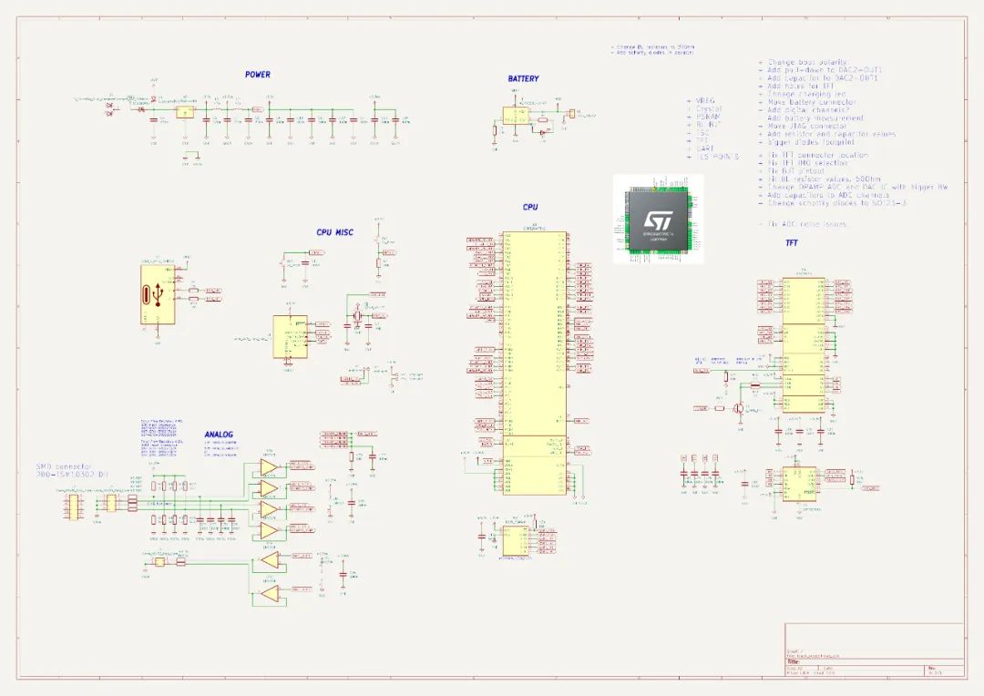
3. Power Supply
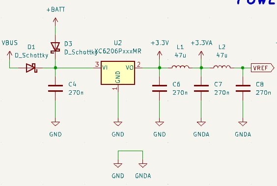
The power subsystem mainly consists of a 3.3V voltage regulator and a LiPo battery charging module. If USB is connected, the entire system is powered via USB while charging the lithium polymer battery. When there is no USB connection, the current is delivered to the voltage regulator through a Schottky diode..
The analog voltage is derived directly from the digital domain and minimally filtered through an inductor. It would be better to power the analog circuit with a separate voltage regulator, but this was not adopted here. The intrinsic advantage of this design lies in the elimination of a symmetric power supply, thus simplifying the bill of materials (BOM).
In this version, the analog and digital ground layers are interconnected, so a separate ground layer is not required. Subsequent versions will explore designs with isolated ground layers to evaluate their effect on noise reduction, especially when measuring small voltage signals.
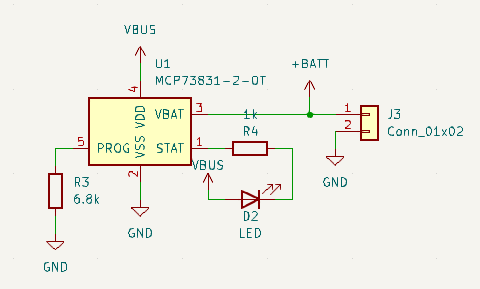
The battery charging module is implemented using a simple SOT23-6 IC, which can easily charge a 130mAh lithium battery. An LED indicator lights up during charging and goes out once completed. The charging cycle takes about an hour, providing approximately two hours of runtime. Although this duration seems limited, we thoughtfully chose a compact battery footprint, and when extended usage time is needed, the oscilloscope can easily connect to a mobile power supply.
The battery-powered voltage is approximately 3.7V, while the circuit’s operating power consumption is around 80mA. Notably, the forward voltage drop measured across the Schottky diode at this current level is about 400mV, imposing a slight limitation on the voltage reaching the voltage regulator. Therefore, future improvements consider integrating two Schottky diodes in parallel to alleviate the current load on each diode and subsequently reduce the voltage drop.
4. Processor
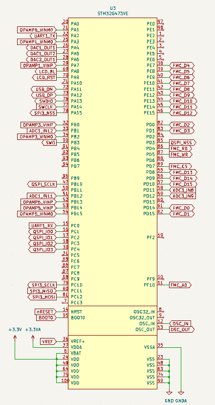
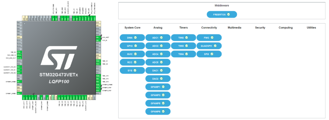
The core of the system is the STM32G474VE, a Cortex-M4F processor running at a clock frequency of 170 MHz. This microcontroller comes in a TQFP-100 package, boasting commendable 512 KB of flash memory and 128 KB of RAM. Currently, the codebase occupies only 20% of the available flash, while operational demands occupy 90% of the allocated RAM. Additionally, the hardware interface utilizes half of the available GPIO pins.
The extensive integration of peripherals inherent in this microcontroller has been a key driver in significantly reducing the bill of materials (BOM). In particular, the inclusion of 4 ADCs has been very helpful. Also noteworthy is the integrated operational amplifier (OPAMP), which exceeds its traditional use by serving as a programmable gain amplifier (PGA) with independent offset inputs. This versatility greatly enhances the system’s functionality, providing a convenient method to adapt to different input conditions.
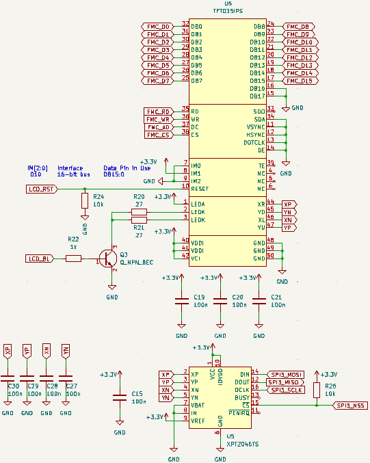
TFT and TSC
The TFT display features an impressive 480×320 pixel resolution and is supported by an ILI9488 controller. It achieves seamless connection with the CPU through a 16-bit 8080 parallel bus, establishing a robust connection for high-speed data transfer.
The CPU utilizes the flexible memory controller (FMC) peripheral to interface with the LCD using a memory-mapped method. This convenient data access method not only accelerates image rendering speeds but also helps achieve a frame rate exceeding 50 FPS. The FMC treats the LCD as a seamless extension of memory, significantly improving data transfer efficiency.
Purchasing the TFT display involves more than just acquiring integrated components from established suppliers like Mouser. Often, pursuing cost-effective solutions on platforms like Amazon or AliExpress can lead to displays lacking comprehensive documentation, including datasheets, pin arrangements, and size specifications. buydisplay.com is a reliable resource for addressing this challenge, offering a variety of displays along with the necessary documentation, thereby simplifying the integration process.
The touchscreen controller (TSC) is connected to the CPU via an SPI bus, capable of efficient operation at a 1 MHz read rate. Throughout the software development phase, it became evident that TSC measurements exhibited a degree of noise, prompting an increase in read frequency for effective filtering. As depicted in the schematic design, initial attempts to mitigate this noise by introducing capacitors in the XP/XN/YP/YN lines yielded uncertain results upon evaluation. This area remains a focus for further study as efforts to optimize noise reduction continue to drive ongoing exploration and refinement.
Two areas for improvement in the design warrant attention. First, the integrated IPS (In-Plane Switching) TFT display is renowned for its superior visual quality and significantly enhanced viewing angles. While these displays can be easily obtained from sources like buydisplay.com, an unfortunate oversight during the procurement process led us to select alternative display technology. This adjustment is expected to significantly enhance the overall user experience, ultimately improving visual fidelity and providing a wider viewing angle.
Another crucial aspect pertains to brightness considerations. Due to the compact battery, the interplay between brightness and battery life becomes particularly pronounced. Increased brightness invariably impacts operational endurance. Therefore, to ensure usage time exceeds one hour, we consciously minimized brightness. Balancing brightness with battery life has become a key task requiring strategic optimization to achieve equilibrium, thereby extending operational time without compromising display visibility.
6. Analog Input and Output Stages
The input stage consists of five different blocks, some of which are integrated within the STM32.
1. Voltage Divider and Low-Pass Filter
The entry point requires a resistor divider network, with a capacitor for each channel. This composite configuration serves multiple purposes, including impedance matching, voltage range adjustment, offset configuration for negative voltages, and high-frequency filtering. This mixture ensures finely processed input signals for subsequent handling.

2. External Operational Amplifier (OPAMP)
A key component in the signal path is the external operational amplifier (OPAMP). By employing TI’s OPA4322, the signal undergoes the necessary conversion, acting as an emitter follower. This operational amplifier has a bandwidth of 20 MHz, exceeding the bandwidth of the input stage, aiding in high conversion rate signal processing without introducing distortion.
3. Internal Operational Amplifier and PGA
After external amplification, the signal enters the integrated operational amplifier and programmable gain amplifier (PGA) unit. These multifunctional components can amplify signals in the range of x2 to x64. This amplification range provides dynamic versatility, allowing the capture of signals from millivolts to volts without the need for external circuits. The combination of the PGA’s external offset input and the use of an additional STM32 DAC avoids any residual offset amplification.
4. Offset DAC
To counteract the offset introduced in the previous stage, a dedicated digital-to-analog converter (DAC) on the STM32 can offset this effect, ensuring signal fidelity and reducing offset distortion.
5. ADC
The final stage requires transmitting the amplified and offset-corrected signal to individual analog-to-digital converters (ADC), each serving a separate channel. This meticulous allocation aids each channel in achieving maximum sampling rates, thereby maintaining signal integrity.
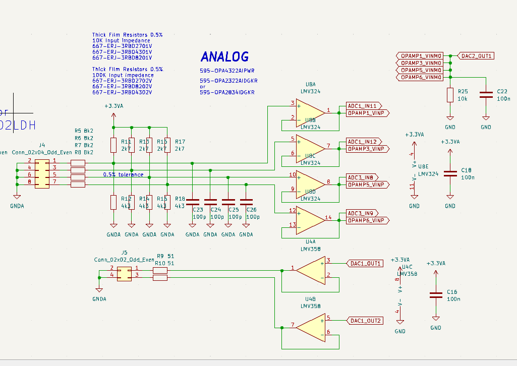
The primary limitation of this design involves the unified offset across all channels. The high tolerances of the input stage resistors may hinder the amplification process of each PGA. To mitigate this issue, the input stage resistors are carefully selected with a precision of 0.5%, ensuring uniform amplification performance.
Additionally, an unexpected challenge arose regarding the pins designated for PGA offset, which simultaneously serve as UART2 pins during ST’s bootloader operation. Rectification is achieved by introducing pull-down resistors and capacitors to maintain a stable DAC voltage during normal operating phases.
Transitioning to the output stage, this arrangement combines the STM32’s DAC, operational amplifiers, and 50-ohm resistors. This synergy enables the generation of various waveforms, including PWM, sine waves, triangular waves, and even arbitration modes, with a maximum frequency of up to 1 MHz, while always limiting to a voltage range of 0 to 3.3V.
Furthermore, the analog signal input section is envisioned to provide four input channels along with the potential for two differential channels. Although not yet verified, the hardware’s infrastructure can accommodate this anticipated expansion.
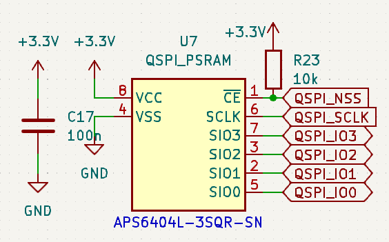
PSRAM Pin Connection Diagram
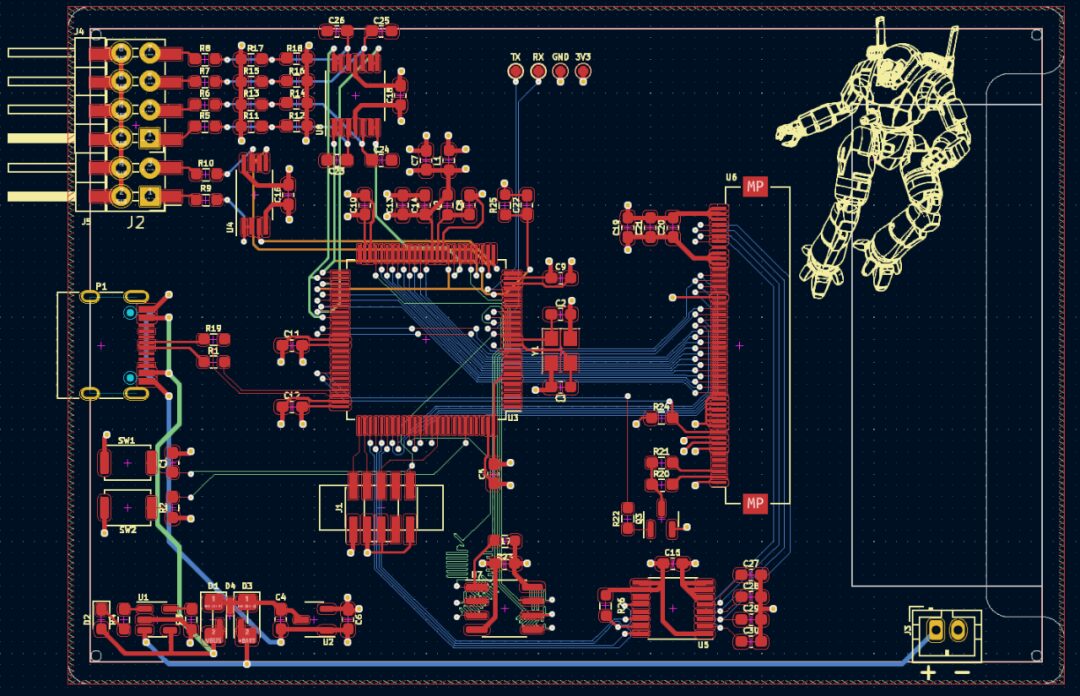
Printed Circuit Board
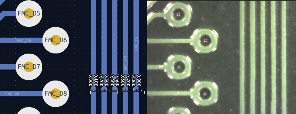
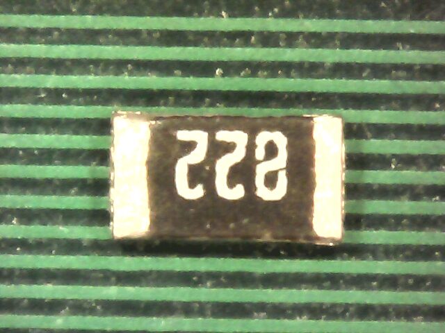
Four-layer PCB
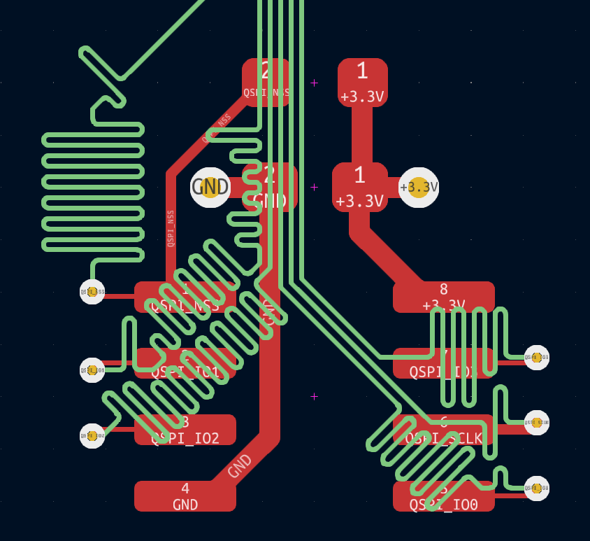
PSRAM Layout
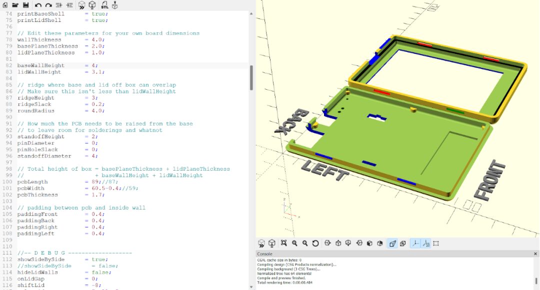
3D Shell Design
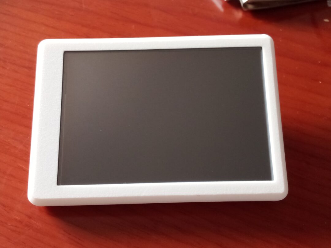
Physical Shell

ADC Collection System
There is also a software introduction; due to space limitations, detailed technical information about this project will not be elaborated here. Interested friends can click at the end of the article “Read Original” to view.

END
→Follow to avoid getting lost←