MAKER: JuanF92/Translated by: Fun Endless Meeting is Just a First Encounter
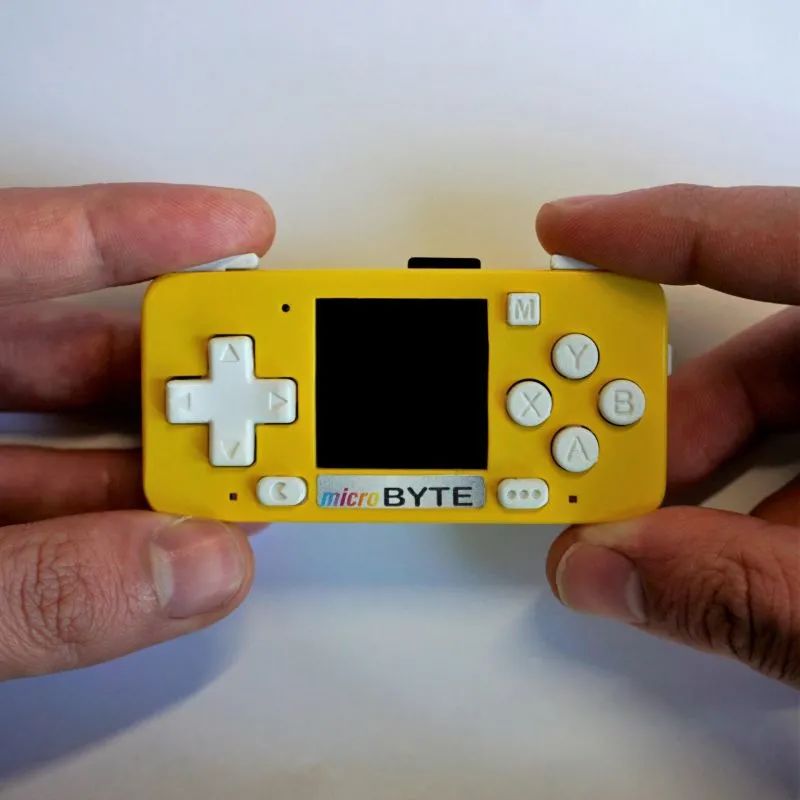
MicroByte is a mini console capable of running games from NES, GameBoy, GameBoy Color, Game Gear, and Sega Master System. All components are designed within this 78 x 17 x 40 mm package. Despite its small size, it conforms to the layout of the SNES game board and features operational buttons. It also comes with a clear 1.3-inch IPS display, allowing you to see all the details of the games.
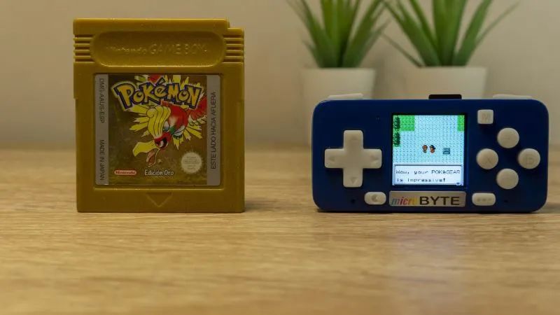
Python and Arduino libraries will be updated for development work beyond gaming.
Firmware, PCB design, 3D files for the casing, etc. can be downloaded from the project repository: https://make.quwj.com/project/359
BOM list: https://github.com/jfm92/microByte_PCB/blob/main/microByte_BOM.xlsx
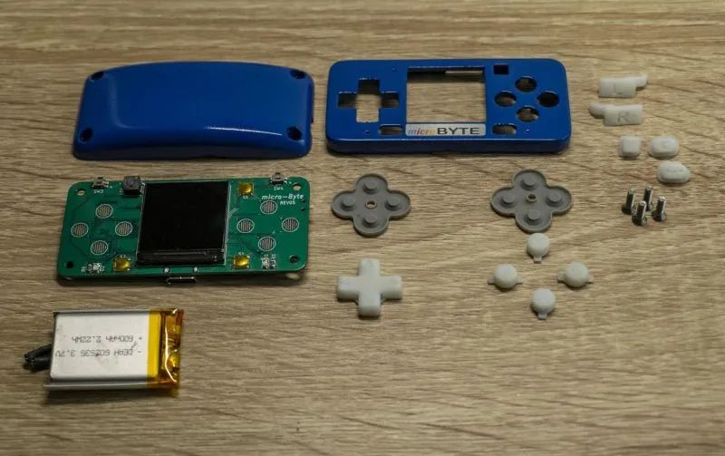
Project Architecture
When starting an electronic project, a block diagram is usually created first, outlining the required functions and interactions for the project, followed by the schematic diagram. On the schematic, components that meet the requirements are selected and electrically connected, followed by PCB layout design. Finally, the position of each component’s footprint is set according to design rules and physical design guidelines.
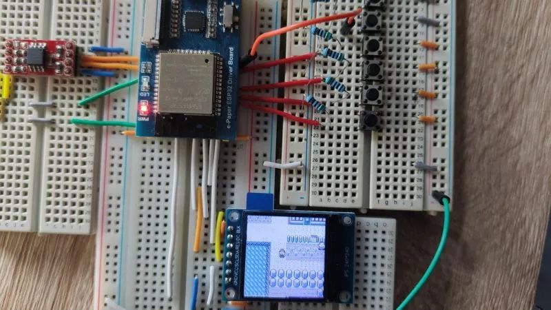
The above is the original version based on a breadboard, and below is the final version.
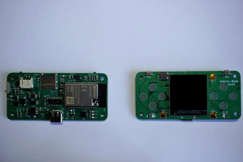
This project will be developed following a modular approach, supplemented by schematic design and PCB layout design.
The project schematic and PCB layout were designed using Kicad, download link: https://github.com/jfm92/microByte_PCB/tree/5cb0fcf7a9658e331d677588a7f35327a7d491d7
To open it, simply install Kicad and double-click the .pro file.
ESP32 Microcontroller
The appropriate microcontroller was chosen first; for this project, the ESP32 Wrover E module was selected. This module/microcontroller features: 240 MHZ dual-core, 16 MB flash memory, 8 MB RAM, ultra-low power co-processor, supports Wi-Fi and Bluetooth, and a full set of peripherals and GPIO, providing excellent emulation performance.
For design reference, please check Espressif’s documentation, the datasheet is as follows: https://www.espressif.com/sites/default/files/documentation/esp32-wrover-e_esp32-wrover-ie_datasheet_en.pdf
The schematic for the board module:
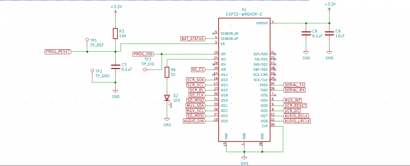
In the middle is the ESP32 module connected to peripherals.
Pin 25 is the IO 0 pin. This pin is for selecting the boot state of the device; it can flash new firmware or boot already flashed firmware. A high signal boots the flashed firmware; a low signal starts the boot mode and waits for new firmware.
Pin 3 is the enable pin (also known as reset). If this pin is high, the microcontroller will work; otherwise, it will not. To avoid signal bouncing, there is an RC circuit (resistor/capacitor) here that generates a clean signal during board startup or transitions to prevent accidental resets. Since there is no reset button in this circuit, it is not entirely necessary, but it’s best to err on the side of caution.
Pin 24 is the IO 2 pin, connected to a blue LED with a resistor, serving as a notification display. Let’s look at pin 2 or VDD 3V3. This pin powers the chip, with a voltage of 3.3 V. Note the parallel capacitors; these capacitors are decoupling capacitors used to eliminate parasitic interference.
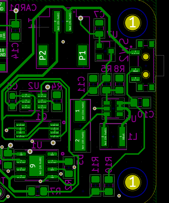
Below is the PCB design layout and key areas of focus in the PCB board.

In addition, related components must be kept as close as possible.
Adding USB Module
The USB transceiver is a chip that converts USB signals to serial, RS232, or other similar protocols. There are various models available on the market, here we use CH340C.
CH340C does not require an external clock like CH340G; it is easy to use and costs just a fraction of the price of CP2102 or FT232.
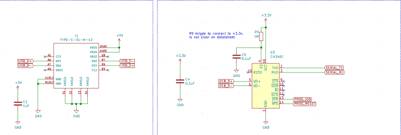
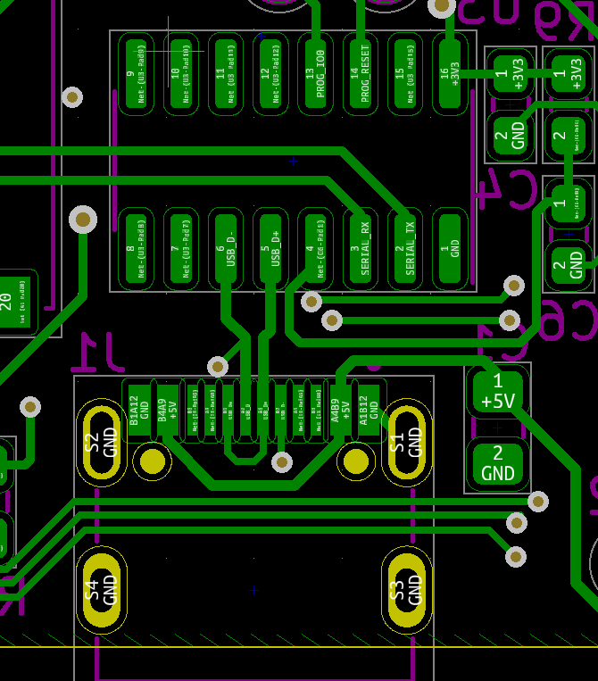
As shown on the right side of the figure. Its design is very simple, consisting of just one chip, two decoupling capacitors, and a 0-ohm resistor. If unsure whether a connection is necessary, this resistor can be used as a bridge.
To the right is a schematic diagram of the USB-C connector. Its purpose is to connect to the PC and charge the battery. When routing on the PCB, using USB-C is more challenging since double connections are needed, allowing wires to be used in any direction.
Tip: USB signals are parallel high-speed signals and should be routed as parallel as possible to avoid crosstalk between signals, and signal lines should be routed close to digital logic chips.

Battery and Power Management
This section is divided into three parts: battery charging and protection circuit, power management, and battery level control. Battery charging and protection circuit:
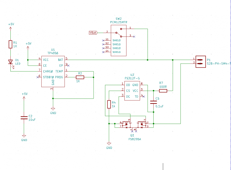
For the use of Li-Po batteries, safety is paramount, requiring a proper constant current charging controller to prevent charging above 4.2 V or discharging below 2.8 V to avoid damaging the battery.
TP4056 is a lithium polymer battery charger chip that provides a constant linear voltage current and can set the charging current by modifying the value of R2. Remember that the charging current should be about 25% of the battery capacity. This chip is connected to LED D1 to indicate the battery’s charging status.
FS312F-G is a battery protection circuit chip that cuts off battery usage if it detects overcharging or over-discharging. This helps to avoid battery damage.
FS8205 is a chip that integrates two MOSFET transistors to select circuit power; if the battery is within the appropriate range, it will draw energy from the battery; if the device is connected to the USB port, it will directly utilize USB power.
Power management:
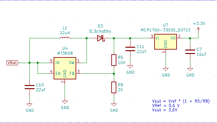
This module is a boost circuit for the voltage converter, providing a constant voltage of 3.3 V. The maximum charging voltage for lithium batteries is 4.2 V, and the minimum safe voltage is 2.8 V. Therefore, a constant voltage is needed to prevent the microcontroller from becoming unstable or the display from being dim. To address this, we use MT3608, a configurable boost voltage converter. At the output of this circuit, the voltage is 4.2 V, which is higher than the 3.3 V required by the device, so we use an MCP1700 voltage converter to convert the voltage from 4.2 V to 3.3 V.
This scheme may have issues with over-design or inefficiency, but it is the cheapest and most effective solution.
Battery level control:
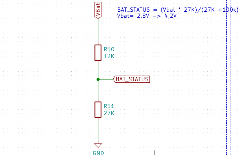
Just like the voltage divider before the boost circuit, this point’s voltage will reach a maximum of 4.2 V, so only a voltage divider needs to be designed to drop to 3.3 V to comply with the ESP32 logic level and connect it to the ADC GPIO to measure the analog level signal.


Designing the SD Card Module
The SD card uses the SPI protocol, which is a bidirectional communication method that enables high-speed communication. When using peripherals, there is no need to worry about crosstalk, as its speed is insufficient to generate a magnetic field (at least there are no issues here).
The circuit is also very simple, connecting each line to the MCU’s SPI GPIO ports and adding a pull-up resistor. This resistor is crucial for maintaining a constant high level on the line and avoiding intermediate level signals that could potentially disrupt data transmission.
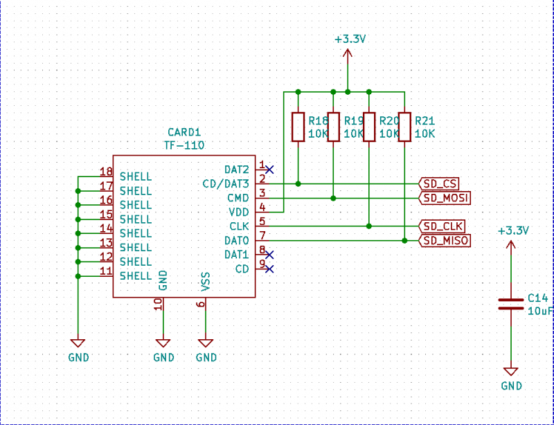
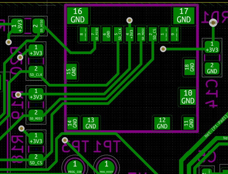
Here we also have our old friend, the decoupling capacitor.
Audio Output
Using the ESP32, there are two ways to output audio. By checking the datasheet, we can use the integrated I2S to DAC converter or directly use the I2S peripheral.
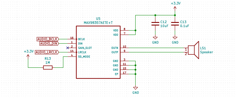
The easiest way to obtain audio output is to use the I2S to DAC converter, as it allows direct connection of the speaker to GPIO. If the audio volume is low, an analog audio amplifier can be used, which is very easy to implement. However, this solution also brings some inconveniences. The DAC only uses 8 bits of the 16 bits of I2S, meaning a lot of audio information is lost, resulting in poor audio quality.
I2S is a digital audio protocol that ensures high-fidelity audio without quality loss or noise. However, it requires a converter to simulate what the amplifier receives. Here we adopt the MAX98357 audio amplifier. This amplifier converts I2S signals to analog signals and amplifies them for direct use with speakers or headphones. This amplifier/converter provides us with 6.4W of output power and has configurable output options—choosing between mono or stereo audio and impedance selection.
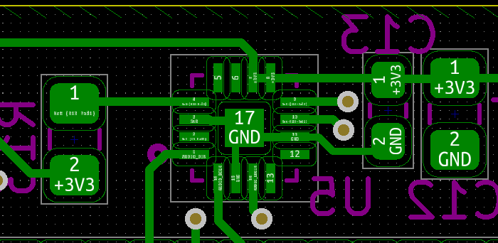

Disclaimer: My understanding of audio is not very deep, so some audio data may be incorrect and is for reference only.
Adding Buttons
The ESP32 is a great module, but it has a limited number of GPIO ports. However, we have the TCA9555 solution.
TCA9555 is an I2C GPIO multiplexer. This device allows for up to 18 additional GPIOs. These GPIOs can be used as inputs or outputs and can be controlled or checked via I2C. Thus, by using just two GPIOs (I2C SDA and I2C SCLK), we have 18 extra GPIOs! Latency is not an issue, as data can be read or written at speeds up to 400 Khz, meaning 400,000 times per second!
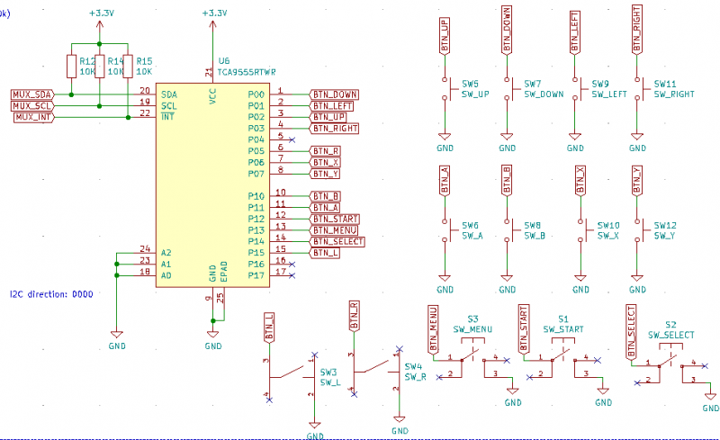
Let’s take a look at the schematic. This multiplexer can be used with I2C, so each signal needs to be pulled up to avoid noise on the lines. It also has an interrupt pin, but it is not used. The I2C signals are SCL and SDA pins (19 and 20). The device’s address needs to be configured through hardware by setting the logic levels of pins A0, A1, and A2. Here, there is only one I2C device, so the address is given as 0x00.
Finally, all switch buttons are directly connected to the chip, and we configured pull-up or pull-down resistors through software, as this multiplexer has configurable internal resistors.
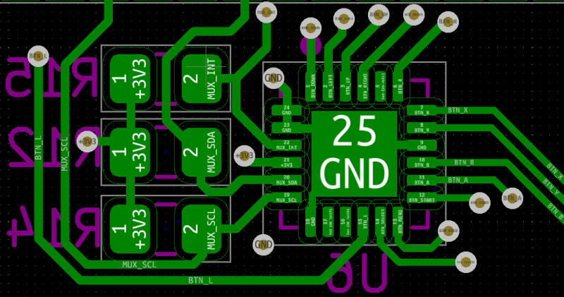
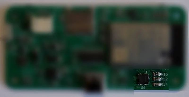
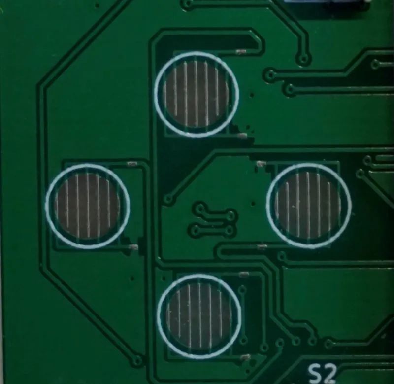
One interesting aspect of this device is the inductive buttons, which are PCB traces without silkscreen layers, so rubber buttons with carbon film can be used as switch buttons. This is the regular configuration on game controllers. If you want to use this in your design, it can be found in the library that accompanies the project.
Pair with a Beautiful Display
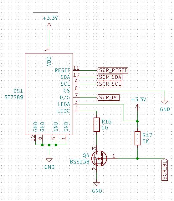
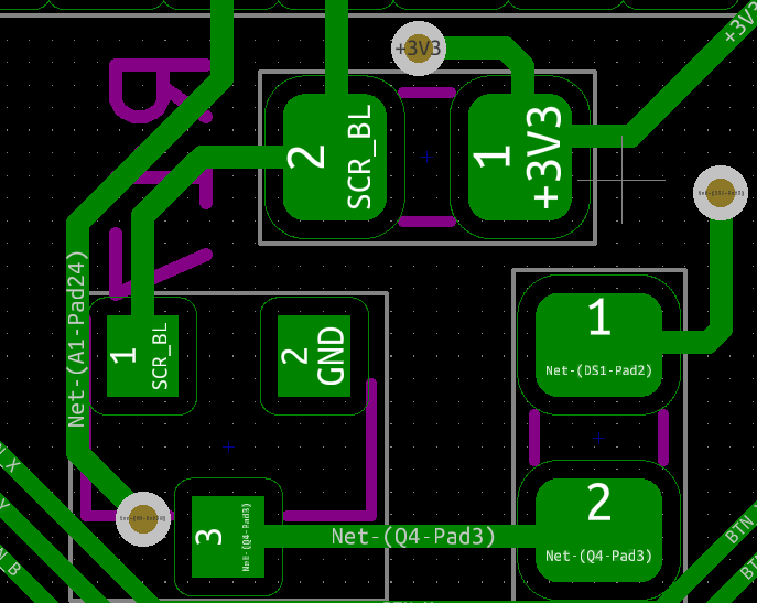
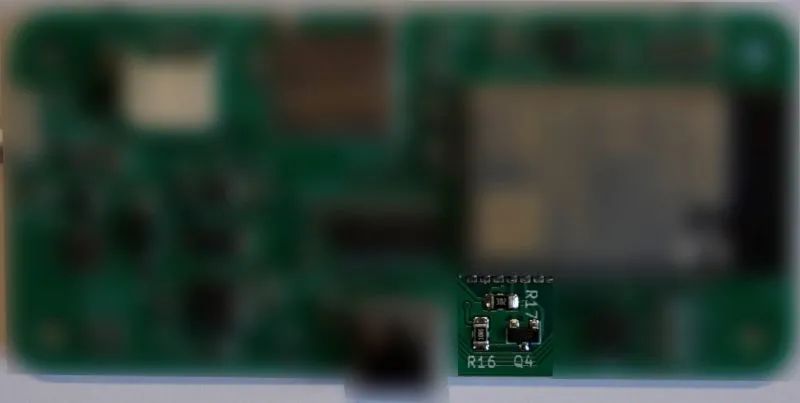
The display uses a 1.3-inch IPS screen with a resolution of 240 x 240 px, providing very nice colors and clear images. The communication protocol is SPI, allowing for a frame rate of up to 70 FPS (as stated in the datasheet). On the other hand, the backlight of the display can be controlled to select brightness levels. This is accomplished by controlling the current of the embedded LED on the display through a BS138 MOSFET transistor.
Completion
You can now run this retro game console and start your nostalgic gaming journey!
The code used for the project can be downloaded from the project repository: https://make.quwj.com/project/359
via instructables.com/MicroByte-DIY-Retro-Console/

Chip Home Selected Article Collection (1): Save it for a Slow Read
Chip Home Selected Article Collection (2): Save it for a Slow Read

