AT89C51 is a low-voltage, high-performance CMOS 8-bit microprocessor with 4K bytes of flash programmable and erasable read-only memory, commonly known as a microcontroller. This device is manufactured using ATMEL’s high-density non-volatile memory technology and is compatible with the industrial standard MCS-51 instruction set and output pins. By combining a multifunctional 8-bit CPU and flash memory on a single chip, ATMEL’s AT89C51 is an efficient microcontroller that provides a high degree of flexibility and a cost-effective solution for many embedded control systems.
Pin Description:
VCC: Supply voltage.
P0 Port: The P0 port is an 8-bit open-drain bidirectional I/O port, each pin can sink 8 TTL gate currents. When the P1 port pin is written as 1 for the first time, it is defined as a high-impedance input. P0 can be used for external program data storage, and it can be defined as the eighth bit of data/address. During FLASH programming, P0 serves as the raw code input, and when FLASH performs verification, P0 outputs the raw code, at which point P0 must be pulled high externally.
P1 Port: The P1 port is an 8-bit bidirectional I/O port with internal pull-up resistors, and the P1 port buffer can receive output of 4 TTL gate currents. After writing 1 to the P1 port pin, it is pulled high internally and can be used as input. When the P1 port is pulled low externally, it will output current due to the internal pull-up. During FLASH programming and verification, P1 serves as the eighth address input.
P2 Port: The P2 port is an 8-bit bidirectional I/O port with internal pull-up resistors, and the P2 port buffer can receive and output 4 TTL gate currents. When a “1” is written to the P2 port, its pin is pulled high by the internal pull-up resistor and serves as input. When used as input, if the P2 port pin is pulled low externally, it will output current due to the internal pull-up. P2 outputs the high eight bits of the address when accessing external program memory or 16-bit address external data memory. When the address “1” is given, it utilizes the advantage of the internal pull-up, and when reading and writing to the external 8-bit address data memory, P2 outputs the contents of its special function registers. During FLASH programming and verification, P2 receives high eight-bit address signals and control signals.
P3 Port: The P3 port pins are 8 bidirectional I/O ports with internal pull-up resistors, which can receive and output 4 TTL gate currents. When writing “1” to the P3 port, they are pulled high internally and used as input. As input, due to external pull-down to low level, the P3 port will output current (ILL) due to the pull-up. The P3 port can also serve as some special function ports of the AT89C51, as shown in the table below:
Pin Alternative Function
P3.0 RXD (Serial Input Port) P3.1 TXD (Serial Output Port) P3.2 /INT0 (External Interrupt 0)
P3.3 /INT1 (External Interrupt 1) P3.4 T0 (Timer 0 External Input) P3.5 T1 (Timer 1 External Input)
P3.6 /WR (External Data Memory Write Enable) P3.7 /RD (External Data Memory Read Enable)
P3 also receives some control signals for flash programming and verification. The pin diagram for the 89C51 is as follows:
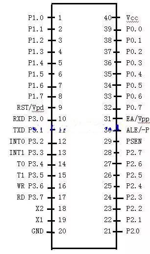
Figure 2-2 89C51 Pin Diagram
RST: Reset input. When the oscillator resets the device, the RST pin must be held high for two machine cycles.
ALE/PROG: When accessing external memory, the address latch enable allows the output level to latch the address byte. During FLASH programming, this pin is used for input programming pulses. Normally, the ALE pin outputs a positive pulse signal at a constant frequency, which is 1/6 of the oscillator frequency. Therefore, it can be used as a pulse for external output or for timing purposes. However, it should be noted that each time it is used as external data memory, one ALE pulse will be skipped. To disable ALE output, set 0 at SFR8EH address. At this point, ALE only takes effect when executing MOVX, MOVC instructions. Additionally, this pin is slightly pulled high. If the microprocessor is in an external execution state, ALE is disabled, and the setting is invalid. To make the modularized automatic bell system more convenient and flexible, we have carefully designed the hardware of the system. The hardware circuit includes three main modules: seven-segment display driver module, buzzer driver module, and button control module.


To facilitate better learning for everyone, Changxue Electronics has specially added a public account focused on microcontrollers and EDA, pushing relevant knowledge daily, hoping to assist your studies!