1. Machine Language
Machine language is a collection of machine instructions, which are commands that a machine can correctly execute. The machine instructions of an electronic computer are a series of binary data, which the computer converts into a series of high and low voltages to drive its electronic components for computation.
2. Assembly Language
1. Characteristics
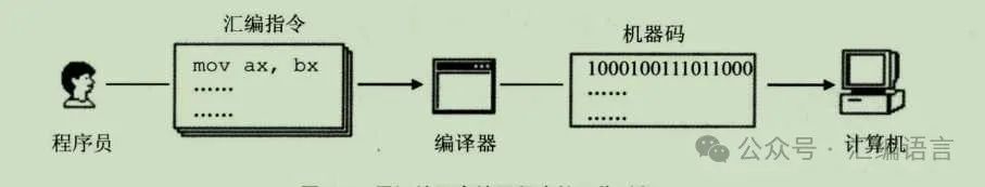
The main body of assembly language consists of assembly instructions, which differ from machine instructions in their representation. Assembly instructions are a more memorable written format.
For example:
Machine instruction: 1000100111011000 indicates sending the contents of the BX register to the AX register.
Assembly instruction: mov ax,bx
Please add a description for the image.
2. Components of Assembly Language
-
Assembly instructions: Mnemonics for machine code, corresponding to machine code.
-
Pseudoinstructions: No corresponding machine code, executed by the compiler.
-
Other symbols: Such as +, -, *, /, etc.
3. Memory
The CPU is the core component of a computer, controlling its operation and performing computations. To enable the CPU to work, instructions and data must be provided, which are stored in memory.
4. Instructions and Data
Instructions and data are merely conceptual applications. In memory or on disk, there is no difference between them; both are binary information. When the CPU operates, it interprets some information as instructions and others as data, attributing different meanings to the same information. Only during use do they hold significance.
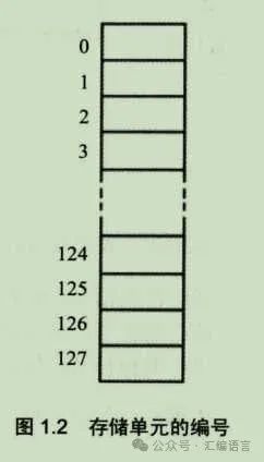
5. Memory Units
Characteristics: Memory is divided into several memory units, each numbered starting from 0. Each memory can store 128 Bytes, while one memory unit can store 1 Byte.
Insert image description here.
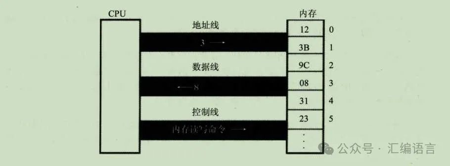
6. CPU Read and Write Operations on Memory
When the CPU needs to read data from memory, it must interact with external devices (chips) through the following three types of information exchange:
-
Address of the memory unit (address information).
-
Device selection, read or write (control information).
-
Data to be read or written (data information).
Electronic calculators can process and transmit information as electrical signals, which require wires for transmission. In computers, there are dedicated wires connecting the CPU to other chips, commonly referred to as buses.
Insert image description here.
-
The CPU sends the address information of memory unit 3 via the address line.
-
The CPU issues a memory read command through the control line, selecting the memory chip and notifying it to read data from it (or write command).
-
The memory sends the data from unit 3 to the CPU via the data line (or sends data to memory unit 3).
How does the CPU perform data reading?
Machine code: 101000010000001100000000
Meaning: Read data from memory unit 3 into register AX.
Assembly instruction: MOV AX,[3]
7. Buses
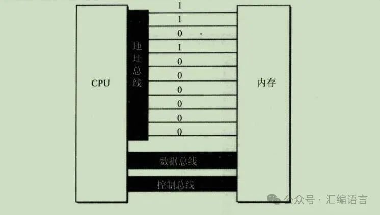
7.1 Address Bus
The CPU specifies memory units via the address bus, meaning the number of different information that can be transmitted on the address bus determines how many memory units the CPU can address.
For example: If a CPU has 10 address lines, and each wire can transmit two stable states: high voltage and low voltage, which correspond to 1 and 0, then 10 binary data can transmit 2 to the power of 10, with the minimum being 0 and the maximum being 1023. If a CPU has N address lines, it can address up to 2 to the power of N memory units.
Insert image description here.
7.2 Data Bus
Data transmission between the CPU and memory or other devices is carried out via the data bus. The width of the data bus determines the data transfer speed between the CPU and the external world. An 8-line data bus can transmit one 8-bit binary data (one byte) at a time, while a 16-line data bus can transmit 2 bytes at once.
The data bus width of the 8088 CPU is 8 bits, while that of the 8086 CPU is 16 bits. Therefore, to transmit the data 89D8 into memory, the 8088 needs to do it in two transmissions.
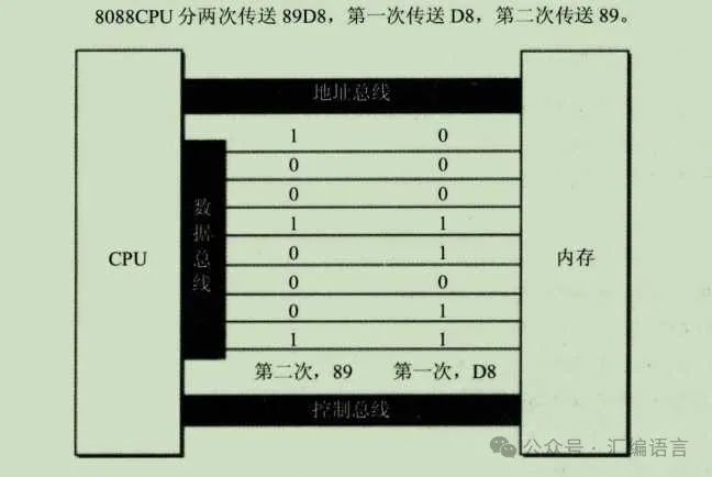
[External image transfer failed, the source site may have anti-leech mechanisms; it is recommended to save the image and upload it directly.]
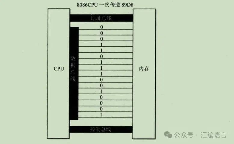
[External image transfer failed, the source site may have anti-leech mechanisms; it is recommended to save the image and upload it directly.]
7.3 Control Bus
The CPU controls external devices through the control bus. The control bus is a collection of different control lines. The number of control lines represents the number of control types the CPU has over external devices. The width of the control bus determines the CPU’s control capability over external devices.
The previously mentioned memory read or write command is issued through several control lines, one of which is called the “read signal output,” and another is called the “write signal output” control line.
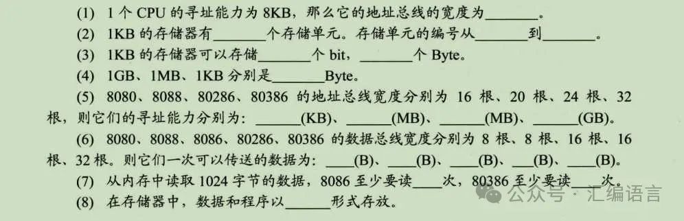
Checkpoints
Insert image description here.
-
16 lines of buses.
-
1024 memory units, numbered 0-1023.
-
8192 bits, 1024 Bytes.
-
1073741824, 1048576, 1024.
-
64, 1, 16, 4 (one memory unit can store 8 bits, 1 byte).
-
1, 1, 2, 2, 4.
-
512, 256.
-
Data.
8. Memory Address Space
For example: If a CPU’s address bus width is 10, then it has 1024 memory units, and these 1024 addressable memory units form the memory address space. For a 64-bit CPU, theoretically, the addressing capacity can reach over 200w TB.
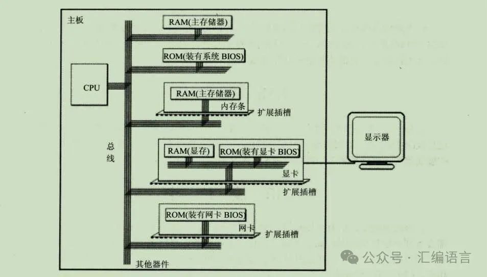
9. Motherboard and Interface Cards
Motherboard: Every PC has a motherboard, which contains core and major components connected via buses. For example: CPU, memory, peripheral chipsets, expansion slots. Expansion slots typically hold RAM memory sticks and various interface cards.
Interface Cards: All devices controlled by programs must be under the control of the CPU. Devices such as monitors and speakers are connected to the CPU through interface cards on expansion slots, and interface cards are connected to the CPU via buses. The CPU can directly control these interface cards to manage external devices.
10. Types of Storage Chips
From the perspective of write attributes, they are divided into two types: Random Access Memory (RAM) and Read-Only Memory (ROM).
RAM: Readable and writable, must be powered to store, and loses content when powered off.
ROM: Readable but not writable, retains content when powered off.
-
Random Access Memory: Stores the vast majority of programs and data for the CPU.
-
ROM with BIOS: BIOS is the software system provided by motherboard and various interface card manufacturers, allowing basic input and output operations using that hardware device.
-
RAM on interface cards: Some interface cards require temporary storage for large amounts of input and output data, which is equipped with RAM. The most typical example is the video memory of graphics cards.
[External image transfer failed, the source site may have anti-leech mechanisms; it is recommended to save the image and upload it directly.]
11. Memory Address Space
When the CPU controls external devices, it treats them all as memory, considering them as a unified logical memory composed of several memory units, which is what we refer to as memory addresses.
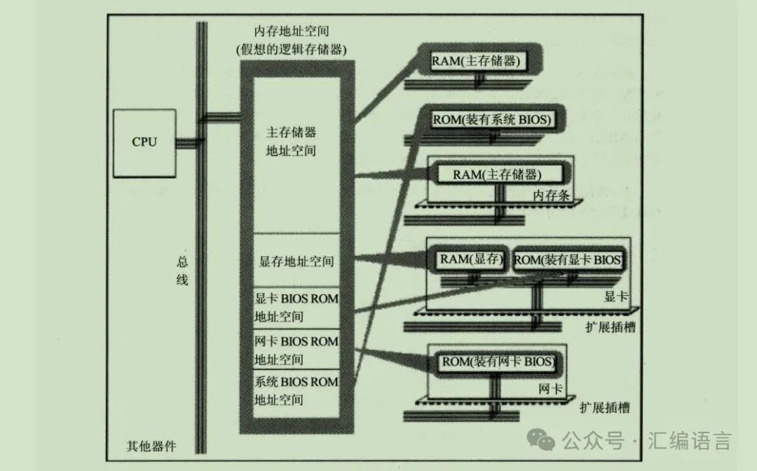
[External image transfer failed, the source site may have anti-leech mechanisms; it is recommended to save the image and upload it directly.]
Assuming the address segments of the memory address space in the above figure are allocated as follows:
-
0 – 7FFFH for the 32KB space of main RAM address space.
-
8000H – 9FFFH for the 8KB space of video memory address space.
-
A000H – FFFFH for the 24KB space of various ROM address spaces.
If the CPU writes data to the memory unit at address 1000H, this data will be written into the main RAM; if it writes data to the memory unit at address 8000H, this data will be written into the graphics card and then output to the monitor.
The size of the memory address space is limited by the CPU’s address bus width. If the bus width is 20, it can transmit 2^20 different address information, which is 1MB; similarly, if the bus width is 32, the maximum memory address space is 4GB. Therefore, when we want to read and write data in a certain type of memory, we must know the address of the first and last units; for example, to display data on the screen, we must know the memory address space of the video memory.
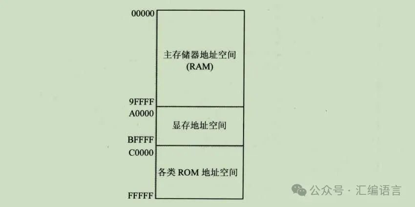
The allocation of memory addresses varies among different calculators. Below is the memory address allocation of the 8086 CPU.
[External image transfer failed, the source site may have anti-leech mechanisms; it is recommended to save the image and upload it directly.]
00000 – 9FFFF corresponds to data in the main memory; A0000 – BFFFF corresponds to data in the video memory; C0000 – FFFFF is invalid as ROM is read-only memory.
Ultimately, the program is run by the CPU, and when we use assembly language, we must consider issues from the CPU’s perspective. All memory units in the system are viewed as a unified logical memory, and its capacity is limited by the CPU’s addressing capabilities.
Published by: Full Stack Programmer Stack Leader. Please cite the source: https://javaforall.cn/179761.html Original link: https://javaforall.cn