1 Silicon Wafers Are Important Semiconductor Materials, With A Scale Exceeding 10 Billion USD
Silicon wafers are the most demanded semiconductor materials
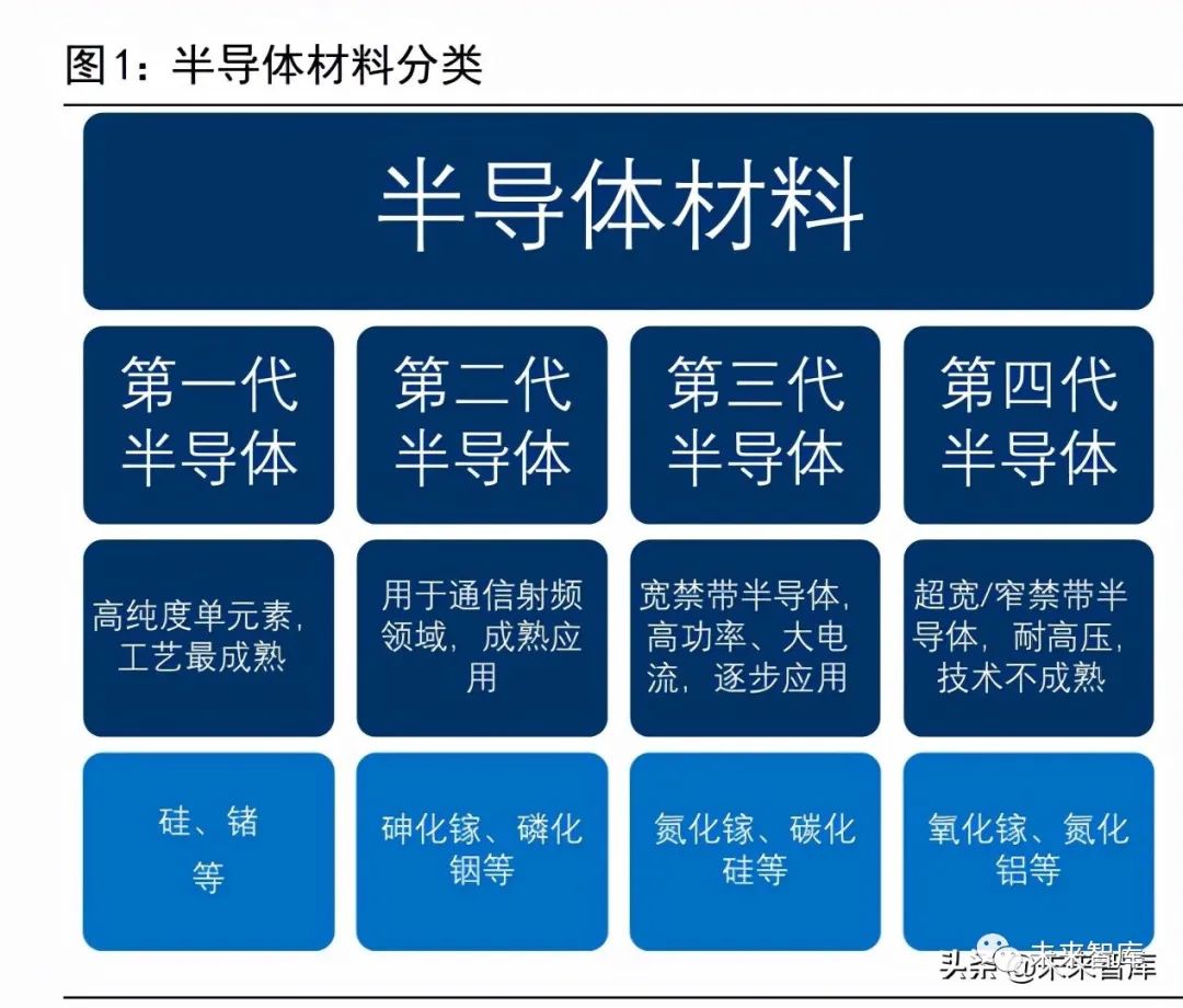
Semiconductor materials are a class of electronic materials that possess semiconductor properties (conductivity between conductors and insulators) and can be used to make semiconductor devices and integrated circuits, forming the foundation of the semiconductor industry. Research on semiconductor materials began in the 19th century and has developed to the fourth generation of semiconductor materials, with each generation complementing the others.
The first generation of semiconductors: represented by silicon (Si) and germanium (Ge), consists of elemental semiconductor materials made from single elements. The development of silicon semiconductor materials and their integrated circuits led to the emergence of microcomputers and a leap in the entire information industry.
The second generation of semiconductors: represented by gallium arsenide (GaAs), indium phosphide (InP), etc., also includes ternary compound semiconductors such as GaAsAl and GaAsP, as well as some solid solution semiconductors and non-static semiconductors. With the rise of information highways based on optical communication and the development of social informatization, second-generation semiconductor materials have shown their superiority. Gallium arsenide and indium phosphide semiconductor lasers have become key devices in optical communication systems, while gallium arsenide high-speed devices have opened up new industries in fiber optics and mobile communications.
The third generation of semiconductors: represented by wide bandgap semiconductor materials such as gallium nitride (GaN), silicon carbide (SiC), and zinc oxide (ZnO). They exhibit excellent properties such as high breakdown electric field, high thermal conductivity, high electron saturation velocity, and strong radiation resistance, making them more suitable for producing high-temperature, high-frequency, radiation-resistant, and high-power electronic devices. They have broad application prospects in semiconductor lighting, next-generation mobile communications, energy internet, high-speed rail transportation, new energy vehicles, and consumer electronics.
The fourth generation of semiconductors: represented by ultra-wide bandgap semiconductor materials such as gallium oxide (Ga2O3), diamond (C), and aluminum nitride (AlN), with a bandgap width exceeding 4 eV; and ultra-narrow bandgap semiconductor materials represented by antimonides (GaSb, InSb). Ultra-wide bandgap materials have more prominent characteristics than third-generation semiconductor materials in high-frequency power devices due to their wider bandgap; ultra-narrow bandgap materials, due to their easy excitation and high mobility, are mainly used in detectors, lasers, and other devices.
Silicon materials manufacture the vast majority of semiconductor products globally and are also the most significant semiconductor manufacturing materials. In the early 1950s, germanium was the primary semiconductor material. However, due to poor high-temperature resistance and radiation resistance of germanium semiconductor devices, it was gradually replaced by silicon materials in the 1960s. Because silicon devices have much lower leakage current and silicon dioxide is a high-quality insulator, it can be easily integrated as part of silicon devices. To this day, semiconductor devices and integrated circuits are still primarily made from silicon materials, which constitute the vast majority of global semiconductor products. According to SEMI data, in the silicon wafer manufacturing process, semiconductor silicon wafers (silicon wafers) are also the largest raw material, accounting for about 38% in 2018.
Classification of Semiconductor Silicon Wafers Based on Different Parameters
Semiconductor silicon wafers (Semiconductor Silicon Wafer) are the foundation for manufacturing silicon semiconductor products and can be classified based on different parameters.
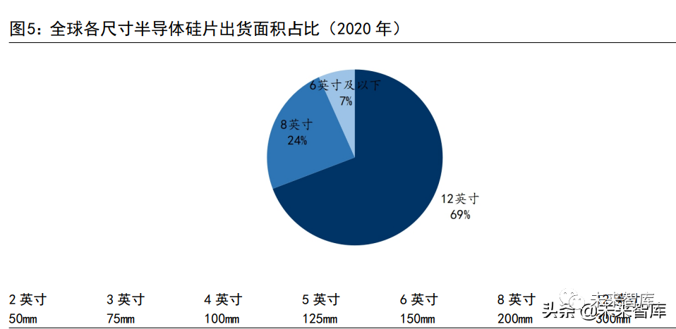
Based on size (diameter), semiconductor silicon wafers can be divided into 2 inches (50 mm), 3 inches (75 mm), 4 inches (100 mm), 5 inches (125 mm), 6 inches (150 mm), 8 inches (200 mm), and 12 inches (300 mm). Under the influence of Moore’s Law, semiconductor silicon wafers are continuously developing toward larger sizes, with 8 inches and 12 inches being the mainstream products, accounting for over 90% of the total shipping area.
Based on doping levels, semiconductor silicon wafers can be classified as lightly doped and heavily doped. Heavily doped wafers have a high amount of doping elements, low resistivity, and are generally used for power devices; lightly doped wafers have a low doping concentration and are generally used in integrated circuits, which have higher technical difficulty and quality requirements. Since integrated circuits account for over 80% of the global semiconductor market, the demand for lightly doped silicon wafers is greater.
Based on processes, semiconductor silicon wafers can be divided into ground wafers, polished wafers, and special silicon wafers such as epitaxial wafers and SOI based on polished wafers. Ground wafers can be used to manufacture discrete devices; lightly doped polished wafers can be used to manufacture large-scale integrated circuits or as substrate materials for epitaxial wafers, while heavily doped polished wafers are generally used as substrate materials for epitaxial wafers. Compared to ground wafers, polished wafers have better surface flatness and cleanliness.
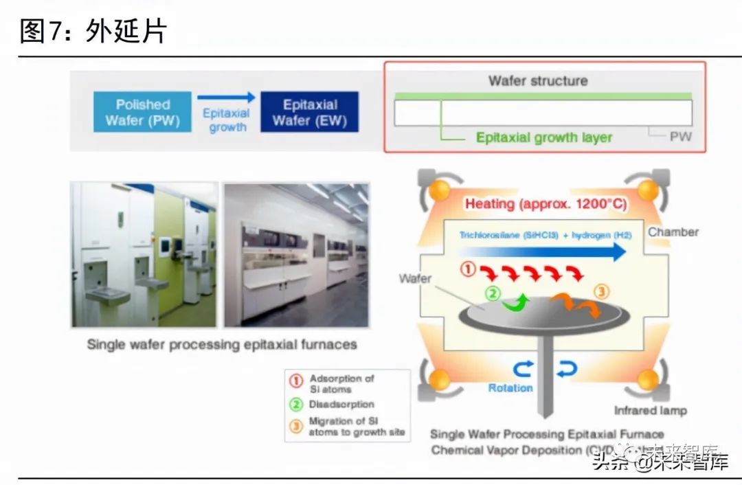
Based on the basis of polished wafers, it is possible to manufacture annealed wafers, epitaxial wafers, SOI silicon wafers, and isolation silicon wafers. Annealed wafers undergo high-temperature heat treatment in a hydrogen or argon environment to remove oxygen near the wafer surface, improving the integrity of the surface crystal. Epitaxial wafers have a layer of single crystal silicon grown by gas-phase growth on the surface of polished wafers, meeting the needs of multi-layer structures with crystal integrity or different resistivities. SOI silicon wafers (Silicon-On-Insulator) insert a high electrical insulation oxide film layer between two polished wafers, achieving high integration, low power consumption, high speed, and high reliability of devices, and can also form arsenic or arsenic diffusion layers on the active layer surface. Isolation silicon wafers are pre-formed IC embedded layers on the wafer surface according to customer design using exposure, ion implantation, and thermal diffusion techniques, and then a layer of epitaxial layer is grown on top.
Based on different application scenarios, semiconductor silicon wafers can be divided into prime wafers and dummy wafers. Prime wafers (Prime Wafer) are used for the manufacture of semiconductor products, while dummy wafers (Dummy Wafer) are used for warm-up, filling gaps, testing the process state of production equipment, or the quality status of a certain process. Dummy wafers are generally cut from the lower quality parts of the crystal rod, and due to the large quantity used, some products may be recycled and reused under certain conditions, with recycled silicon wafers being called reclaimed wafers (Reclaimed Wafer). According to data from the Research Institute, a 65 nm process wafer foundry requires 6 dummy wafers for every 10 prime wafers, while for processes at 28 nm and below, 15-20 dummy wafers are required for every 10 prime wafers.
The Semiconductor Silicon Wafer Industry Is Cyclical, With A Market Size Of 12.6 Billion USD In 2021
The market size of semiconductor silicon wafers fluctuates with the prosperity of the global semiconductor industry, and the unit area price rose after hitting the bottom in 2016. According to SEMI data, global semiconductor silicon wafer sales increased from 7.9 billion USD in 2005 to 12.6 billion USD in 2021, with the shipping area increasing from 6.645 billion square inches to 14.165 billion inches. The unit area price first fell and then rose, decreasing from 1.19 USD/inch in 2005 to 0.67 USD/inch in 2016, and then rebounding to 0.89 USD/inch in 2021. As the most important raw material for semiconductor products, the fluctuation direction of the global semiconductor silicon wafer market size is basically consistent with global semiconductor sales, and the fluctuation range is larger, showing significant cyclicality.
2 The Manufacturing Process Of Semiconductor Silicon Wafers Is Complex, With High Industry Barriers
The Manufacturing Process Of Semiconductor Silicon Wafers Is Complex, With Crystal Pulling Being A Key Step
The upstream of semiconductor silicon wafers is semiconductor-grade polysilicon material, and the downstream is semiconductor products. Silicon elements exist mainly in nature in the form of silicon dioxide, which is chemically reduced to produce polysilicon material, which is then purified. The purity requirement for photovoltaic polysilicon material is between 6 to 9 nines (99.9999%-99.9999999%), while the purity requirement for semiconductor use is above 11 nines (99.999999999%). The completed semiconductor silicon wafers are used by wafer fabs as substrates to manufacture various semiconductor products, which are finally applied in terminal products such as mobile phones and computers.
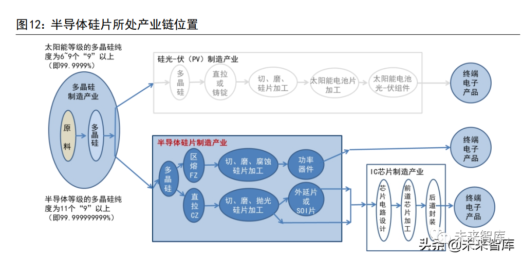
The manufacturing process of semiconductor silicon wafers is complex and mainly includes crystal pulling and processes such as slicing, grinding, polishing, and epitaxy. The production process of semiconductor silicon wafers is complex and involves many steps. The grinding wafer process includes crystal pulling, cutting, rounding, slicing, chamfering, and grinding. Polished wafers are manufactured based on grinding wafers through edge polishing, surface polishing, and other processes; polished wafers are used to produce silicon epitaxial wafers through epitaxy processes, and silicon annealed wafers are produced through annealing heat treatment. Special processes are used to produce silicon SOI (Silicon-On-Insulator). The silicon wafer manufacturing process requires multiple cleaning steps, and before being sold to customers, it must also undergo inspection and packaging.
Step 1: Crystal Pulling. High-purity polysilicon is pulled into single crystal silicon rods through single crystal growth processes. Common methods include the Czochralski method (CZ method) and the Float-Zone method (FZ method). The FZ method has high purity, low oxygen content, high resistivity, and can withstand high pressure, but has high difficulty in processing, making it difficult to prepare large-size silicon wafers and expensive, thus mainly used for 8-inch and smaller sizes, primarily for medium to high-end power devices. The CZ method has higher oxygen content, is easier to produce large-size single crystal silicon rods, and is a mature process with lower costs; therefore, the semiconductor industry mainly uses the CZ method to pull single crystal silicon rods. The crystal pulling technology directly determines the density of dislocations, COP (crystal originated pits), and other native crystal defects, as well as the quality of key technical indicators such as resistivity, resistivity gradient, and oxygen and carbon content, making it the core technology in the production process of semiconductor silicon wafers. (Report Source: Future Think Tank)
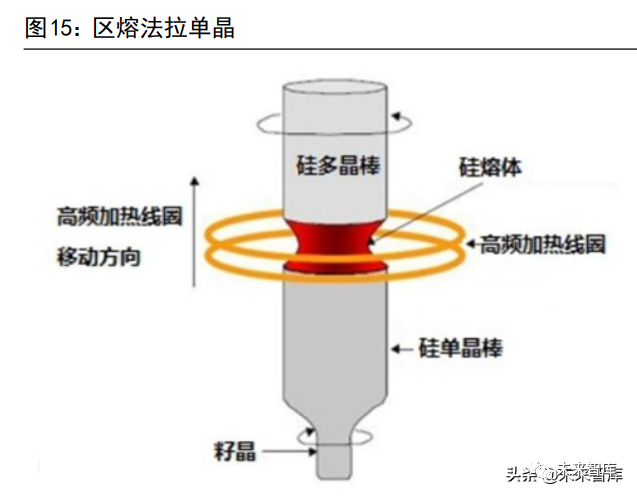
Czochralski Method Processing Technology:
Loading: Place polysilicon and dopants into the quartz crucible of the single crystal furnace. The type of dopant depends on the desired resistivity, mainly including boron for growing P-type and phosphorus, arsenic, and antimony for growing N-type.
Melting: After loading, heat to above the silicon melting temperature (1420°C), melting the polysilicon and dopants, allowing them to evaporate for a certain period, then lowering the seed crystal to approach the liquid surface, preheating the seed crystal for a few minutes, commonly known as “baking the crystal” to remove volatile impurities on the surface while reducing thermal shock.
Seed Crystal Pulling: Once the temperature stabilizes, bring the seed crystal into contact with the melt, then lift the seed crystal upward at a certain speed while maintaining a certain rotation speed. As the seed crystal rises, silicon crystallizes at the head of the seed crystal, called “seed crystal pulling” or “seeding”.
Necking: After pulling the seed crystal, slightly lower the temperature and increase the pulling speed to pull a section that is narrower than the seed crystal diameter. The purpose is to eliminate polycrystalline caused by poor contact and to minimize the extension of existing dislocations in the seed crystal. The neck should generally be longer than 20 mm.
Shoulder Formation: After the necking process is completed, gradually reduce the lifting speed and temperature to adjust the crystal diameter to the desired size. During shoulder formation, it can be determined whether the crystal is single crystal; otherwise, it must be melted and re-seeded.
Constant Diameter Growth: When the crystal diameter reaches the desired size, increase the pulling speed so that the crystal diameter no longer increases, known as shoulder reduction. After shoulder reduction, maintaining a constant diameter means constant diameter growth. At this point, strict control of temperature and pulling speed is required. Single crystal silicon wafers are taken from the constant diameter section.
Ending: After completing the constant diameter section, if the crystal rod is immediately separated from the liquid surface, the stress will cause dislocations and slip lines in the crystal rod. To avoid this problem, the diameter of the rod must be gradually reduced until it forms a point and separates from the liquid surface.
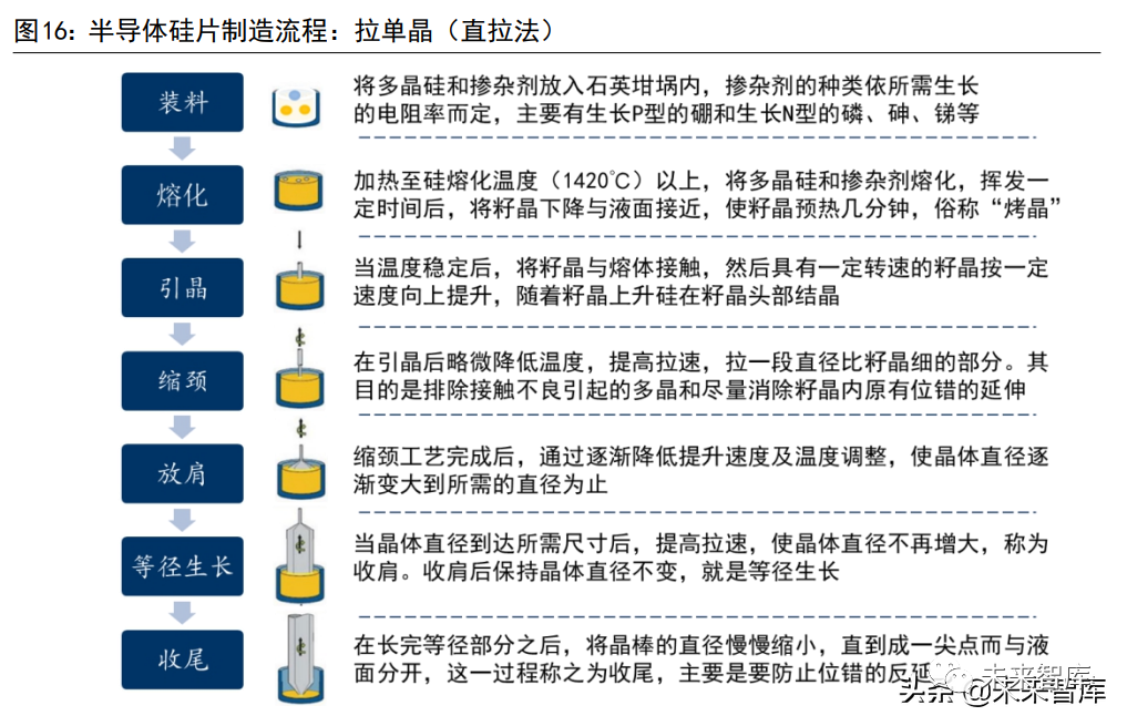
Float-Zone Method Processing Technology:
Step 1: In a vacuum or rare gas environment, use an electric field to heat the polysilicon rod until the polysilicon in the heated area melts, forming a molten zone. Bring the seed crystal into contact with the molten zone and melt it. The molten zone on the polysilicon continuously moves upward, while the seed crystal slowly rotates and is pulled down, gradually forming a single crystal silicon rod.
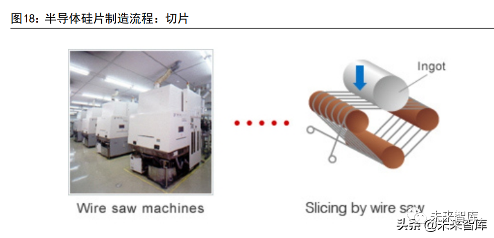
Step 2: Slicing. The single crystal silicon rod is ground to the same diameter, then sliced into thin sheets about 1 mm thick according to the customer’s required resistivity using an inner diameter saw or wire saw to form wafers. Based on current processes and technology levels, to reduce silicon material loss and improve production efficiency and surface quality, wire cutting methods are generally used for slicing.
Step 3: Chamfering: The purpose of chamfering silicon wafers is to eliminate edges, cracks, burrs, chipping, or other defects and various edge surface contaminations caused by cutting processing, thereby reducing the roughness of the edge surface and increasing its mechanical strength, reducing surface contamination of particles.
Step 4: Grinding. Use abrasives on a grinder to polish the slices to the required thickness while improving surface flatness. The purpose of grinding is to remove the surface mechanical stress damage layer of about 20-25 μm caused during the slicing process and various metallic ion contaminations on the surface, ensuring a certain level of flatness on the wafer surface.
Step 5: Etching and polishing. Chemical etching is used to remove mechanical damage caused to the wafer surface in the previous steps, followed by mechanical-chemical polishing using silicon sol to make the wafer surface even smoother and shinier.
Step 6: Cleaning and inspection. After cleaning, the products undergo strict quality inspections, and once approved, they are sold to customers. They can also be further used to produce SOI, epitaxial wafers, and other special silicon wafers.
The Semiconductor Silicon Wafer Industry Has High Barriers, With First-Mover Advantages And Scale Effects Prominent
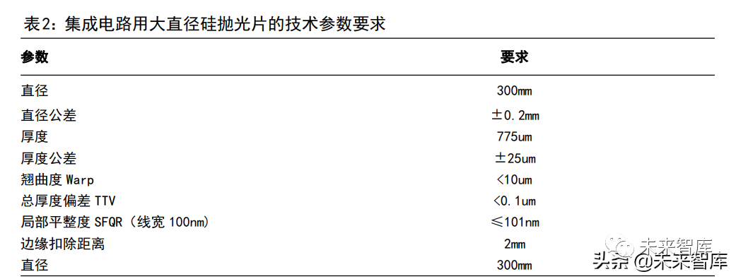
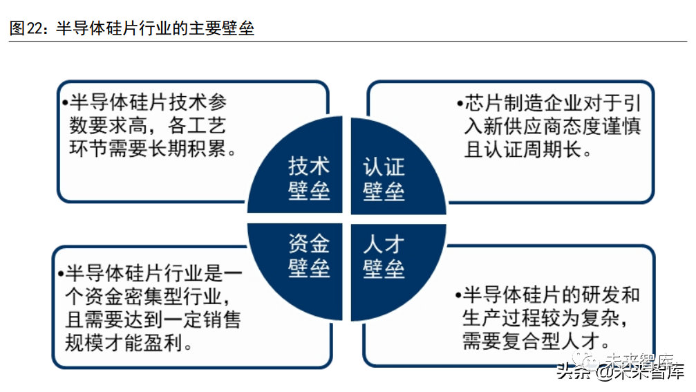
Technical Barriers: Semiconductor silicon wafer technology parameters are highly demanding, requiring long-term accumulation in various process links. Core processes of semiconductor silicon wafers include single crystal processes, slicing processes, grinding processes, polishing processes, epitaxy processes, etc., with a high degree of technical specialization. The single crystal process is the most core technology, determining the size, resistivity, purity, oxygen content, dislocations, and crystal defects of the wafers. In the single crystal growth process, temperature control and pulling rate are crucial. Wafer grinding and polishing processes determine the thickness, surface flatness, cleanliness, particle size, and warpage of the wafers. The key to the epitaxy process is ensuring the uniformity of the epitaxial layer thickness and the uniformity of the epitaxial layer resistivity within the wafer.
Customer Certification Barriers: Chip manufacturing companies are cautious about introducing new suppliers, and the certification cycle is long. Semiconductor silicon wafers are important raw materials for chip manufacturing companies in producing semiconductor products. Chip manufacturing companies are cautious about introducing new suppliers to ensure the stability and consistency of product quality, requiring a long certification cycle. Typically, chip manufacturing companies require silicon wafer suppliers to first provide some wafers for trial production. After passing internal certification, the products will be sent to downstream customers for approval, and only then will they certify the silicon wafer suppliers and formally sign procurement contracts.
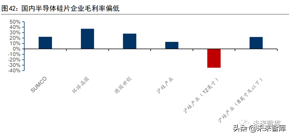
Financial Barriers and Scale Barriers: The semiconductor silicon wafer industry is capital-intensive and requires a certain sales scale to be profitable. Significant investment is required to achieve scaled production of semiconductor silicon wafers, with the cost of key production equipment reaching tens of millions of yuan. The investment amount for large-size silicon wafer production lines is in the billions. Additionally, due to the high initial fixed asset investment, semiconductor silicon wafer companies need to achieve a certain scale of sales before they can be profitable, leading to significant operational pressure in the early stages, with gross margins potentially negative.
Talent Barriers: Semiconductor silicon wafer companies require composite talents. The R&D and production processes of semiconductor silicon wafers are complex, involving interdisciplinary fields such as solid-state physics, quantum mechanics, thermodynamics, and chemistry, thus requiring composite talents with comprehensive professional knowledge and rich production experience.
3 12-Inch Demand Exceeds Supply, International Environment Accelerates Domestic Substitution
The Development History Of Semiconductor Silicon Wafers: Originating In The USA, With Japan Catching Up Later
Semiconductor silicon wafers originated in the USA, with MEMC leading technology development and achieving numerous global firsts. The semiconductor industry originated in the USA, and so did semiconductor silicon wafers. In 1956, the Monsanto Chemical Company established the MEMC Electronic Materials Company, responsible for producing silicon wafers for transistors and rectifiers. Over the following decades, MEMC made significant contributions to industry technology development and industry standards, including breakthroughs in chemical mechanical polishing (CMP), epitaxial layer growth, zero-dislocation crystals, and oxygen control; the company was also the first in the world to mass-produce 4-inch and 8-inch silicon wafers. As an industry leader, MEMC held an 80% market share in the 1960s. However, due to continuous losses later, Monsanto sold MEMC to a German chemical company in 1989, which was subsequently acquired by Taiwan’s GlobalWafers in 2016.
With the rise of domestic semiconductors, Japanese silicon wafer manufacturers have caught up, and companies from South Korea and Taiwan have also gained a foothold in the global market. In the late 1950s, Japanese companies began to layout the silicon wafer industry through technology introduction. Driven by the Very Large Scale Integration (VLSI) research program (1976-1980), the Japanese semiconductor industry developed rapidly, with memory surpassing the USA in the 1980s. During this period, silicon wafer manufacturers experienced a golden development period, eventually consolidating and merging into two international semiconductor silicon wafer giants: Shin-Etsu Chemical and SUMCO. In 2001, Shin-Etsu Chemical was the first in the world to mass-produce 12-inch semiconductor silicon wafers. Since surpassing the USA in the 1990s, the Japanese semiconductor silicon wafer industry has maintained a dominant position globally. In the 1990s, the semiconductor industry shifted from Japan to South Korea and Taiwan, allowing silicon wafer companies in these regions to grow and gain a foothold in the global market.
Competitive Landscape: Strong Domestic Supply and Demand, Market Concentration Expected to Decrease
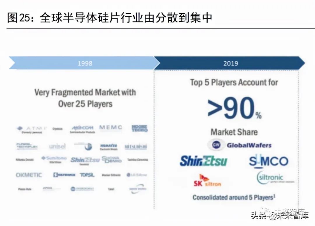
The development of the semiconductor silicon wafer industry has been accompanied by consolidation and acquisitions, with the competitive landscape shifting from fragmented to concentrated. The early development of the semiconductor silicon wafer industry was dominated by the USA’s MEMC, followed by numerous companies entering the competition. In 1998, the market landscape was extremely fragmented, with over 25 major market participants worldwide. However, as wafer sizes increased, the required investment significantly increased, making scale effects key to profitability. Continuous losses among many wafer manufacturers have led to ongoing acquisitions and mergers. Through continuous consolidation, the global semiconductor silicon wafer industry has shifted from fragmentation to concentration, with the top five silicon wafer manufacturers accounting for over 90% of the market share in 2019.
The international environment accelerates domestic substitution, and global market concentration is expected to decrease. In the context of tense international relations, semiconductor supply chain security has become a focus for governments and companies worldwide. As core raw materials, semiconductor silicon wafers are in strong domestic demand. In 2022, Taiwan’s GlobalWafers’ acquisition of Germany’s Siltronic was announced to have failed due to not obtaining German regulatory approval. Under the supply influence of domestic semiconductor silicon wafer manufacturers, the competitive landscape of the semiconductor silicon wafer industry is expected to change, and global market concentration is likely to decrease. According to SEMI data, the combined market share of the top three global semiconductor silicon wafer manufacturers decreased from 68.2% in 2019 to 63.8% in 2020; the combined market share of the top five manufacturers decreased from 92.6% to 86.6%.
Increased Demand for 8-Inch and 12-Inch Wafers, Stable Demand for Small Size Wafers
The increase in semiconductor content drives the increase in wafer shipping area, with global wafer shipments reaching a historical high in 2021. Historically, the average annual growth rate of the semiconductor industry has been higher than that of the overall electronic system market, primarily driven by the increasing semiconductor content used in electronic systems. For instance, as the shipment volumes of global mobile phones, automobiles, and personal computers mature and slow down, the average annual compound growth rate of the electronic system market from 2011 to 2021 was 3.5%, while the semiconductor industry achieved a 6.5% average annual compound growth rate during the same period. According to IC Insights data, the semiconductor content in electronic systems reached 33.2% in 2021, a historical high, with an expected final value exceeding 40%. Driven by the increase in semiconductor content, the shipping area of wafers has shown an upward trend. According to SEMI data, the global shipping area of wafers reached 14.165 billion square inches in 2021, setting a historical record.
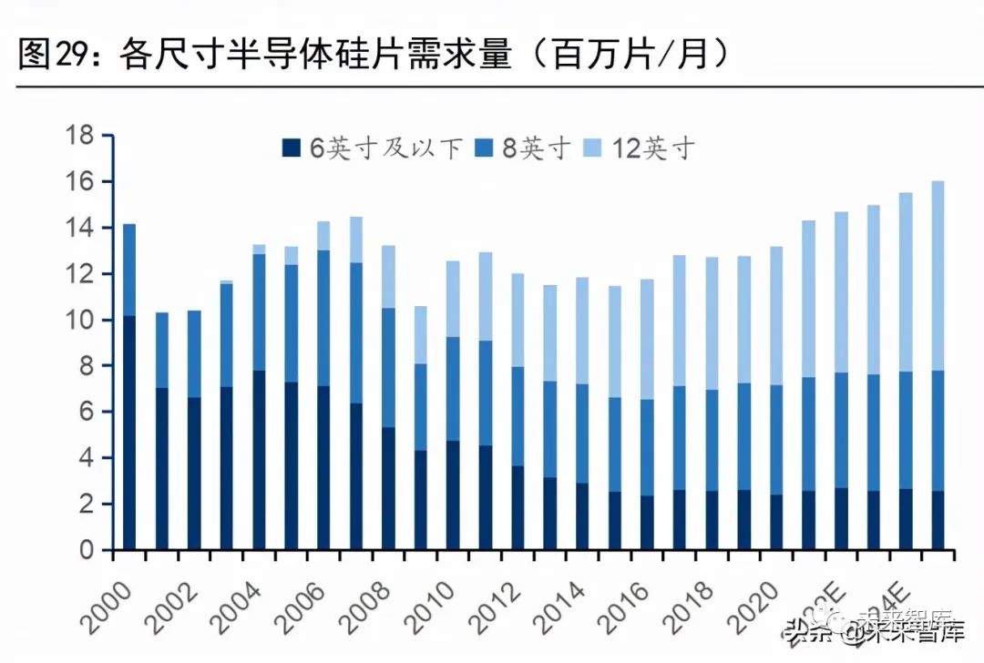
The new demand for semiconductor silicon wafers is concentrated in 8-inch and 12-inch sizes, while demand for 6-inch and smaller wafers remains stable. According to Omdia data, the demand for 6-inch and smaller semiconductor silicon wafers showed a declining trend between 2000 and 2015, remaining stable after 2015; demand for 12-inch wafers has continuously risen since its commercial production in 2001; demand for 8-inch wafers has remained relatively stable. Omdia predicts that from 2021 to 2025, demand for 8-inch and 12-inch semiconductor silicon wafers will increase, while demand for 6-inch and smaller wafers will remain stable. In terms of shipment volume, 12-inch wafers accounted for 47.7% in 2021, 8-inch wafers accounted for 34.3%, and small wafers accounted for 18.0%; in terms of shipping area, 12-inch wafers accounted for 70.9% in 2021, 8-inch wafers accounted for 22.6%, and small wafers accounted for 6.5%.
For cost considerations, discrete devices continue to use small sizes, while integrated circuits are migrating to larger sizes. Due to lower prices, manufacturers of discrete devices have less motivation to invest in large-size production lines, and currently, they still mainly use 6-inch and smaller wafers. The economic benefits of using large-size silicon wafers for integrated circuits are significant. For example, a 12-inch wafer has an area 2.25 times that of an 8-inch wafer and a usable area about 2.5 times that of an 8-inch wafer, increasing the number of chips produced per wafer and subsequently lowering the cost per chip. If the cost savings from increasing wafer size can compensate for the investment in large-size wafer manufacturing lines, manufacturers will have the motivation to migrate to larger sizes. Currently, the largest commercially available semiconductor silicon wafer size is 12 inches, while 18-inch (450 mm) wafers have not yet shown potential for mass production due to process and technical difficulties.
Strong Demand for 12-Inch Semiconductor Silicon Wafers, Short Supply Expected to Last Until 2026
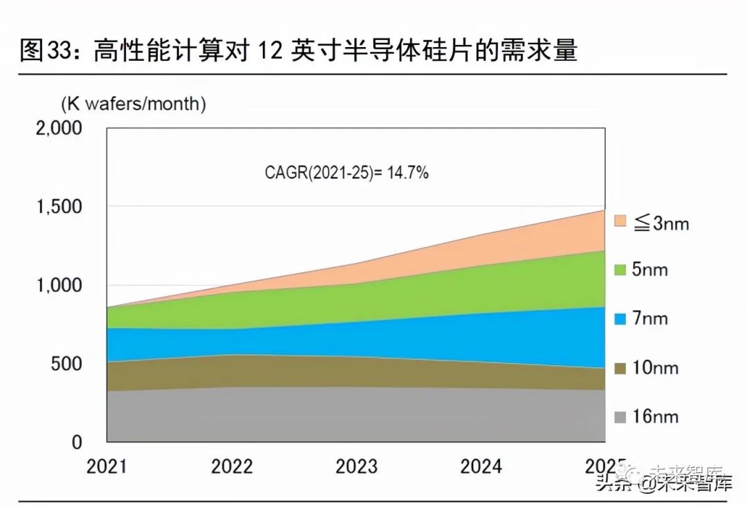
New demands such as remote work, automotive semiconductors, and the metaverse are driving increased demand for 12-inch semiconductor silicon wafers. According to SUMCO’s February 2022 forecast, demand for 12-inch semiconductor silicon wafers will increase due to new demands such as remote work, online meetings, autonomous driving, and the metaverse, with global data volume expected to rise from 13ZB per year to 160ZB, leading to strong demand for data computation and storage. SUMCO expects the CAGR for 12-inch semiconductor silicon wafers demand from high-performance computing and DRAM to be 14.7% and 10%, respectively, from 2021 to 2025.
Downstream wafer fabs are actively investing to expand capacity, increasing demand for 12-inch semiconductor silicon wafers. To meet downstream terminal demands, wafer fabs are increasing capital expenditures to expand capacity, with total investment expected to reach about 150 billion USD in 2022. Third-party foundries are particularly active in advanced processes, with a CAGR of 8.1% from 2020 to 2025, while IDM’s CAGR is 4.6%. With high capital expenditures, the global demand for 12-inch polished wafers is expected to increase from 3.751 million pieces/month in 2020 to 5.554 million pieces/month in 2025, and demand for epitaxial wafers is expected to increase from 2.292 million pieces/month to 2.682 million pieces/month; the required amount of 12-inch wafers for foundries is projected to increase from 1.593 million pieces/month in 2020 to 2.748 million pieces/month in 2025.
The pace of capacity expansion lags behind the increase in demand, leading to a shortage of 12-inch semiconductor silicon wafers. According to SUMCO’s latest forecast in February, the CAGR for 12-inch wafer demand from 2021 to 2026 is expected to be 8.4%. Since large-scale production of new 12-inch wafer plants will not take place until 2024, the supply gap for 12-inch wafers in 2022 and 2023 will be larger than in 2021, with the capacity utilization rate of global 12-inch wafer manufacturers expected to remain above 100% from 2022 to 2026. Additionally, the shortage of 8-inch and smaller wafers is expected to continue in 2022. Based on this, major semiconductor silicon wafer manufacturers are expected to raise prices again in 2022 after the price increase in 2021.
SUMCO’s significant capacity expansion will meet long-term demand, and GlobalWafers announced expansion plans after its acquisition failure. SUMCO has signed long-term contracts with customers for 5 years from 2022 to 2026, and to meet customer demand, SUMCO plans to invest 228.7 billion yen (approximately 12.5 billion RMB) in new plants in Imari and Omura. This is the first investment in new factories since 2008. The two new plants will start construction in 2022 and begin production in the second half of 2023, reaching full production in the second quarter of 2025 and the end of 2023, respectively. These new capacities will be included in the long-term contracts. After the failure of GlobalWafers’ acquisition of Siltronic, they also announced expansion plans in February 2022, intending to invest 100 billion NTD (approximately 22.8 billion RMB) from 2022 to 2024 to expand existing plants and build new factories, with the new production lines expected to start production in the second half of 2023.
4 Strong Supply and Demand for Domestic Semiconductor Silicon Wafers, Domestic Giants Accelerating Rise
Domestic Investment in Wafer Fab Construction Creates Opportunities for Local Semiconductor Silicon Wafer Manufacturers
China is the country with the most new wafer fabs, increasing demand for 8-inch and 12-inch wafers. According to SEMI’s projections, numerous wafer fabs will come online between 2020 and 2024, including 25 8-inch wafer fabs and 60 12-inch wafer fabs. Among them, China has the highest number of new additions, with 14 new 8-inch and 15 new 12-inch fabs in mainland China, while Taiwan has added 2 new 8-inch and 15 new 12-inch fabs. In terms of new 8-inch wafer fabs, mainland China far exceeds other countries/regions. In 2021 and 2022, mainland China added 5 and 3 new fabs, respectively, and the commissioning of new wafer fabs will drive demand for semiconductor silicon wafers.
To Seize Industry Opportunities, Domestic Semiconductor Silicon Wafer Manufacturers Are Actively Expanding Production
Driven by policy and funding, domestic semiconductor silicon wafer companies are investing in production expansion. Developing the semiconductor industry has become a national strategy, with national and local governments increasing support policies. At the same time, under the trend of domestic substitution, a large amount of capital has flooded into the semiconductor industry. With both drivers, the domestic semiconductor industry has entered a period of vigorous development, and semiconductor silicon wafers, as key raw materials, have seen various manufacturers announce investment expansion plans. The construction of semiconductor silicon wafer plants is diverse, with regional dispersion. As domestic large-size semiconductor silicon wafer enterprises are in their early development stages, a monopoly has not yet formed. Various companies and local governments are actively constructing wafer fabs to seize development opportunities, presenting a pattern of multiple construction entities and regional dispersion. From the development history of Japan’s semiconductor silicon wafer industry, in the early stages of industry development, multiple projects progressed simultaneously; as the industry matured, mergers and consolidations became the optimal choice based on scale effects and profitability considerations.
The Domestic Semiconductor Silicon Wafer Industry Is Facing Unprecedented Development Opportunities
Compared to overseas semiconductor silicon wafer companies, domestic companies entered the semiconductor silicon wafer industry later, with large-scale production lagging by over ten years. For instance, the overseas mass production time for 8-inch semiconductor silicon wafers was 1984, while China’s Liangwei’s mass production time was 2009; the overseas mass production time for 12-inch semiconductor silicon wafers was 2001, while China’s Shanghai Xinsheng’s mass production time was 2018. Due to the late start, domestic semiconductor silicon wafer companies face high barriers to entry in the industry, including financial barriers, talent barriers, technical barriers, certification barriers, and scale barriers. However, with national policies and capital support, financial barriers have been largely resolved; at the same time, a favorable entrepreneurial environment and treatment have attracted excellent overseas talents to return and local talents to join, establishing a talent pipeline in the semiconductor silicon wafer field.
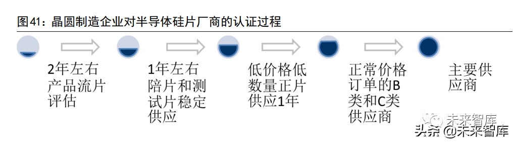
Domestic customers are accelerating validation, with some companies having crossed the certification barriers. New semiconductor silicon wafer manufacturers generally require over 5 years of certification processes to become major suppliers to customers: about 2 years of product trial evaluation—about 1 year of stable supply of dummy and test wafers—1 year of low-price, low-quantity orders of prime supply—B-class and C-class suppliers for normal price orders—major suppliers. To ensure product quality, wafer fabs are generally reluctant to introduce new silicon wafer suppliers in the presence of mature suppliers. However, in the context of tense international relations, domestic wafer manufacturing enterprises have increased their demand for local silicon wafers, becoming more willing to provide certification opportunities for domestic companies. Against this backdrop, some domestic silicon wafer enterprises have successfully completed certification and entered the bulk supply stage. With the accumulation of experience, domestic companies will have more opportunities to introduce overseas customers.
The profitability during the initial mass production phase is weak, but is expected to improve as scale increases. The semiconductor silicon wafer industry requires significant fixed asset investment, making losses easy to incur before achieving scale shipments. Scale effects are one of the competitive advantages for enterprises. Domestic companies have entered the market for a shorter time, and scale effects have not yet formed, leading to weaker profitability in the early stages, especially for 12-inch production lines. For example, in 2020, the overall gross margin of Shanghai Silicon Industry was 13.10%, with a gross margin of 21.76% for products of 8 inches and smaller, while the gross margin for 12-inch products was -34.82%. As capacity and sales ramp up, scale effects will help improve the profitability of enterprises.
Core equipment is gradually being localized, with some manufacturers establishing equipment design capabilities. Building a silicon wafer production line requires a series of equipment, including single crystal furnaces, polishing and cleaning equipment, slicing and grinding equipment, inspection equipment, and epitaxy equipment. Although the production equipment for 12-inch lines is still primarily imported, some domestic equipment has entered production lines. Additionally, the ability to design and modify equipment is also one of the core competencies of semiconductor silicon wafer enterprises. For example, the single crystal furnaces of Shin-Etsu and SUMCO are designed and manufactured independently by the companies or through their holding subsidiaries; other major silicon wafer manufacturers also have their independent single crystal furnace suppliers, bound by strict confidentiality agreements. After years of development, some domestic manufacturers have also established core equipment design capabilities, with Shanghai ChaoSilicon, for instance, having an equipment technology center where core equipment single crystal furnaces are designed and manufactured independently. (Report Source: Future Think Tank)
The Mid-Long Term Outlook for China’s Semiconductor Industry Is Upward, Bringing Investment Opportunities for the Silicon Wafer Industry
The performance and market value of semiconductor silicon wafer companies are strongly correlated with the industry cycle, and signing long-term contracts helps mitigate performance fluctuations. A review of the historical performance of SUMCO, a major global semiconductor silicon wafer manufacturer, shows that the company’s performance and market value fluctuate in line with each other. The period from 2016 to 2018 was an upward phase, while 2019 and 2020 were downward phases. GlobalWafers experienced a similar situation during the 2016-2018 period, with significant improvements in gross margin and net margin, as well as a substantial increase in market value; however, during the downward cycle of 2019 and 2020, GlobalWafers signed long-term contracts with fixed prices and quantities, resulting in smaller fluctuations in gross margin and net margin. Additionally, GlobalWafers made two acquisitions in 2016, including the fourth-largest semiconductor silicon wafer manufacturer globally, leading to a tenfold increase in its market value from 2016 to 2018, far exceeding SUMCO; at the end of 2020, GlobalWafers began planning to acquire Siltronic, which was announced to have failed in early 2022.
In the context of domestic substitution, China’s semiconductor industry has entered a golden development period, bringing investment opportunities for the silicon wafer industry. Amidst tense international relations, the entire Chinese semiconductor industry is entering a period of favorable development, with the outlook expected to continue to improve in the mid-long term as wafer fabs enter expansion phases. According to the revised “Wassenaar Arrangement” at the end of 2019, some high-end semiconductor silicon wafer-related technologies are subject to export controls. Given supply chain security considerations, domestic wafer fabs are increasingly cooperative in adopting domestic silicon wafers. According to the prospectus of Maersk, only about 10% of 8-inch wafers and the domestic supply of 12-inch wafers has just begun. Based on the development history of Japan, South Korea, and Taiwan’s semiconductor silicon wafer industries, the growth of semiconductor silicon wafer companies occurs alongside the rise of the domestic semiconductor industry, and they will undergo a period of consolidation and integration. We believe that the trend of domestic chip production will help cultivate semiconductor silicon wafer companies that hold a position in the global market, making this an opportune time to invest in the semiconductor silicon wafer industry.
Source: DT Semiconductor


Long
Notes
Get More Exciting Content

“New Material Think Tank” is the WeChat public platform of the Strategic Research Center of the Iron and Steel Research Institute. The Strategic Research Center of the Iron and Steel Research Institute is a permanent office of the National Expert Advisory Committee on New Material Industry Development and is also one of the research institutions supported by the Ministry of Industry and Information Technology, the Ministry of Science and Technology, and the State-owned Assets Supervision and Administration Commission. Relying on strong research strength and leading talent advantages, under the leadership of academicians and experts, it has become a member unit of the MIIT Think Tank Alliance and the Central Enterprises Think Tank Alliance, and a technology service organization for military-civilian integration of the Ministry of Industry and Information Technology. It provides strategic consulting, technology information retrieval, industry analysis, market research, and industrial planning services for government departments, research institutions, and domestic and foreign enterprises; participates in the planning and document preparation of new material-related projects by the Ministry of Industry and Information Technology and the Ministry of Science and Technology; undertakes major and key strategic consulting projects of the Chinese Academy of Engineering; formulates industrial development plans for local governments; prepares product development plans for numerous enterprises and provides market research services.
Contact Us
Phone: 01062185650 (same as fax)
Lian Haiqiang: 18514253969 (same as WeChat)