
This article references the “ODCC-2022 Enterprise-Level SSD Technology and Application Report”, covering the overall situation of enterprise-level SSD storage, analysis of innovative technologies for enterprise-level SSDs, analysis of testing technologies for enterprise-level SSDs, and analysis of controller manufacturers.
1. Controller
(1) ARM Architecture
The ARM architecture adopts the ARM instruction set system, developing differentiated processor architectures based on different application scopes. The ARM architecture uses a reduced instruction set (RISC) design, which effectively reduces chip complexity through high clock frequency and short cycle execution of the instruction set. The Load/Store instruction architecture allows the processor to access memory data based on Load and Store instructions. RISC architecture processors include various registers for storing instructions and data, and the ARM architecture is no exception. Although ARM processors do not use single-cycle instructions, most instructions are designed with fixed lengths to facilitate instruction decoding. During computation, the CPU only processes data within the registers. In addition to the ARM instruction set, the ARM architecture also supports 32-bit or 16-bit Thumb instruction sets, which provide stronger code density and work in conjunction with the ARM instruction set to further enhance processor performance. Compared to the complex instruction set (CISC) of the x86 architecture, the ARM architecture effectively improves the execution efficiency of commonly used operations.
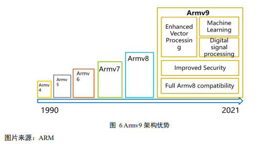
The Armv9 architecture focuses on artificial intelligence, security, and dedicated processing, greatly enhancing overall performance to support tasks such as machine learning, digital signal processing, image, and speech recognition. Armv9 supports Aarch32 and Aarch64 instructions, NEON, cryptographic extensions, and TrustZone. Building on Armv8, it introduces scalable vector extension 2.0 (SVE2), Arm Confidential Computing Architecture (CCA), tracing and debugging, and transactional memory extensions (TME). SVE2 adds fixed-point operations in some Arm supercomputer cores, with vector lengths of 128bit, scaling up to 2048bit, targeting dedicated DSP and XR (augmented and virtual reality) workloads, applied in various fields such as 5G, genomics, and computer vision. The Arm Confidential Computing Architecture (CCA) consists of domain management extensions (RME) and the Arm Confidential Computing Firmware Architecture, establishing a new secure hardware environment while simplifying hardware design and enhancing the scalability, reusability, and portability of confidential computing. The branch record buffer extension (BRBE) for tracing and debugging provides information analysis capabilities for debugging and optimization. The embedded tracing extension (ETE) and tracing buffer extension (TRBE) improve the tracing capabilities of Armv9. The transactional memory extension (TME) supports the hardware transactional memory (HTM) of the Arm architecture, solving high-concurrency writing and multi-threaded programming issues, and enabling coarse-grained and thread-level parallelism to scale with the increase in CPU numbers.
(2) Cortex Processors
The Cortex processors consist of the Cortex-A series, Cortex-R series, and Cortex-M series, providing differentiated functions for different task requirements. The Cortex-A series processors are designed for devices performing complex computational tasks, commonly used in enterprise-level and data center IT equipment. To maintain a balanced performance, power consumption, and size for Cortex-A processors, a front-end processor must be installed, which enhances performance on the Cortex-R processors. The Cortex-R series processors are optimized for high performance, meeting real-time processing and low latency requirements, commonly used in enterprise-level SSDs, consumer SSDs, and data centers. The Cortex-M series is used for discrete processing and microcontrollers, achieving low latency and real-time capabilities through rapid data movement. Low-power consumer controllers often choose this type, but processors like Cortex-M55, Cortex-M33, and Cortex-M0+ can assist SSDs. The Cortex processor series is shown in Table 3.
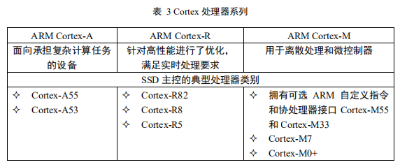
The Cortex-A55 is Arm’s most powerful and efficient mid-range processor, based on DynamIQ technology, suitable for complex computational tasks in enterprise-level SSDs and data center equipment. The Arm Cortex-A55 processor utilizes DynamIQ technology, Armv8-A extension architecture, and dedicated machine learning instructions, forming part of the first generation of CPU applications. The Cortex-A55 employs a redesigned microarchitecture system, significantly improving processor performance and forming strong competitiveness in specifications and energy efficiency. Compared to the Cortex-A53, its performance has improved by 18%, and power efficiency has increased by 15%. As a scalable CPU, the Cortex-A55 can be used to address various application scenarios from edge to cloud computing. The Cortex-A55 can be implemented in standalone applications or as a “shrink” version of the Cortex-A7x series CPUs.
The Cortex-R series processors can effectively support enterprise-level SSD controllers, meeting high real-time and complex task requirements. The Cortex-R5 processor provides extended fault containment for real-time applications. The Cortex-R5 processor enhances error management, functional safety, and SoC integration performance based on the Cortex-R4, suitable for deeply embedded real-time systems and critical safety systems. The Cortex-R8 is the most powerful real-time processor in this series, using a 32-bit instruction set core based on the Armv7-R architecture, 11-stage pipelines, and superscalar out-of-order execution, capable of scaling from single-core to quad-core configurations, fully releasing workload parallelism. The single-core Cortex-R8 can also be powered down based on workload. The Cortex-R82 implements a 64-bit Armv8-R AArch64 architecture processor, accelerating machine learning workloads through Arm Neon technology while using an optional memory management unit (MMU) to support complex operating systems (OS), suitable for data centers, enterprise-level SSDs, and compute storage drives (CSD).
2. Firmware
(1) Firmware Algorithms
Firmware is an important component for enhancing enterprise-level SSD performance. Efficient and high-quality firmware algorithms can improve firmware performance, achieving perfect compatibility between flash memory and controllers, enhancing overall SSD performance. Firmware algorithms consist of various algorithms such as garbage collection, wear leveling, bad block management, data retention, and power loss recovery. Since the same physical block cannot be erased indefinitely, it is necessary to migrate valid data from existing physical blocks to free blocks through garbage collection, reclaiming invalid data that has been written or marked for deletion, and erasing entire block data to make it available again. Wear leveling includes both dynamic wear leveling and static wear leveling. The dynamic algorithm prioritizes writing new data to less worn physical blocks, while the static algorithm migrates cold data to more worn physical blocks, thus freeing writable space. In bad block management, bad blocks, which are physical blocks with read/write/erase exceptions, need to be managed and marked. Bad block management algorithms typically use skip strategies or replacement strategies. Regarding data retention, data stored for too long may experience charge leakage, and multiple reads of physical pages can interfere with surrounding page data, requiring data retention algorithms to monitor physical block data, migrating blocks that exceed the ECC set threshold or the physical page read count threshold to other physical blocks. Power loss recovery addresses power loss that occurs when physical pages are not fully written. The power loss recovery algorithm uses the method of writing the mapping table to flash memory, allowing the retrieval of the previous mapping table in case of power loss.
(2) Error Correction Algorithms
The technical capability of error correction algorithms is key to improving the overall level of enterprise-level SSDs, making the enhancement of algorithm research and design capabilities crucial. LDPC (Low-Density Parity-check Codes, low-density parity check codes) coding is a commonly used soft information coding technology for enterprise-level SSDs, capable of extending lifespan and preserving data for a longer time. The ratio of user data to parity data will differ from before; it is related to signal-to-noise ratio and UBER, not simply a fixed bit error correction. Regarding LDPC error correction codes, to optimize error correction performance and codec algorithm effects, attention needs to be paid to the LDPC parity-check matrix. During design, it is necessary to lower the error floor to a level that does not affect system performance, reduce the complexity of encoding and decoding algorithms, while controlling chip power consumption, system performance, and manufacturing costs. In terms of encoding and decoding algorithms, as the read/write counts of flash memory particles increase, a higher error rate can occur. This can be addressed by upgrading the LDPC codec module’s corresponding interface protocol to extend the usage cycle and establishing an adaptive adjustment mechanism for the decoding algorithm process, completing the decoding task with minimal power consumption and lowest latency.
ECC technology has gradually become an effective way to enhance the core competitiveness of enterprise-level SSDs and ensure performance. As NAND technology continues to iterate and the number of bits per unit increases, the data error rate also increases. Improving SSD error correction capabilities and error correction algorithm technical capabilities has become an important direction for enhancing SSD performance.
(3) Telemetry
Telemetry is a technology that can remotely collect data in real-time from physical or virtual devices. Telemetry enables comprehensive monitoring and assessment of the health of devices, networks, protocols, overlays, and services, generating visual results to quickly locate network faults and assist operations personnel in solving network maintenance issues. Compared to traditional network monitoring methods, this technology is not only fast but also intuitive, providing important technical support and overall solutions for intelligent and refined network operations.
The introduction of Telemetry attributes in SSD products, through customized Extend SMART logs, covers three major categories of attributes related to wear, failure operation counts, and internal abnormal states. In terms of wear-related attributes, these include NAND-level read/write volumes, the wear degree of internal SSD blocks, etc., which can be used to detect SSD faults caused by wear. In failure operation count attributes, these include counts of internal read/write and erase failures, reflecting the reliability of NAND data storage within the SSD. In terms of internal abnormal attributes, these include internal temperature overheating, buffer overflow, etc., caused by load and external environment, reflecting the stability of the internal working state of the SSD.
Through monitoring multiple dimensions of the internal state of the SSD, a comprehensive understanding of the health status of internal components is achieved. Monitoring is more comprehensive, with records for each hardware component of the SSD; records are more detailed, with more detailed records for temperature, etc.; fault logs are more detailed; and closer to the application layer, with more detailed records for various workloads. By introducing Telemetry, the prediction accuracy of faulty disks can be further improved, and the efficiency of intelligent operations and maintenance for data center cloud storage systems can be greatly enhanced.
3. Flash Memory
(1) QLC Technology
QLC SSDs, with their large capacity and low cost, can enhance storage density and server integration. Compared to HDDs, QLC SSDs have a more significant advantage in random read performance, bringing lower read latency to servers and data centers. The technical difficulty of large-capacity QLC SSDs is lower than that of HDDs, generating less heat than HDDs, faster random speeds, stronger shock resistance, and higher capacity density per unit volume. QLC SSDs are suitable for data-intensive applications that require higher real-time data reading, such as AI computing, machine learning, real-time financial data analysis, and various online big data information mining. Meanwhile, QLC has a clear cost advantage compared to flash memory chips such as SLC, MLC, and TLC. In scenarios with massive data applications, the cost competitiveness of QLC SSDs has won them more application scenarios in the data center field. The rapid growth in storage demand has driven the expansion of application ranges for new high-capacity, high-density flash memory chips like QLC SSDs, greatly saving data center space and reducing operating costs.
QLC can provide greater storage space for 3D NAND, suitable for read-intensive workloads, while TLC has stronger write performance and lower error rates. Compared to 2D NAND, 3D NAND offers higher density, enabling more write and erase cycles. Since QLC NAND SSDs can store 4 bits of data per cell, with 16 voltage states, while TLC NAND SSDs can store only 3 bits of data, with 8 voltage states.
In terms of read performance, compared to QLC NAND, TLC requires longer erase cycles and program durations due to fewer bits written per cell, while QLC NAND SSDs have sequential read speeds comparable to TLC SSDs, making them more suitable for read-intensive workloads.
In terms of 3D NAND write performance, TLC SSDs outperform QLC SSDs. Although both technologies use error correction algorithms to ensure data integrity, this process will take more processing cycles on QLC-based drives, severely affecting write performance. TLC and QLC will present a complementary and collaborative development trend. In the future, 50% of NAND flash will be 3D QLC, with the remaining majority being 3D TLC. Additionally, QLC NAND will gradually replace some TLC NAND, and these two technologies will advance together.
(2) SLC Cache Technology
SLC Cache avoids the slowdown problem of high-density storage, providing writing performance, storage capacity, and cost advantages for TLC SSDs or QLC SSDs. SLC Cache essentially simulates SLC operating modes using TLC, QLC, and other particles, marking multiple operating states according to SLC’s two states, simplifying control difficulty while improving speed and durability. The acceleration strategies of SLC Cache include dynamic capacity and fixed capacity types. Dynamic capacity SLC Cache refers to planning SLC Cache based on remaining capacity. For large-capacity SSDs, it can achieve large cache redundancy. However, as the hard disk occupancy increases, overall performance declines, which poses higher requirements for controller intelligence. However, with the growth of SSD capacity, the dynamic drop issue is greatly alleviated.
(3) Xtacking Technology
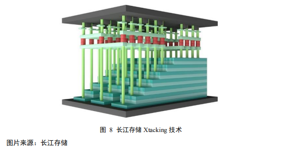
Xtacking technology innovates 3D NAND flash memory, resulting in faster speeds, higher density, and more flexible architecture. Xtacking allows for the separate processing of peripheral circuit wafers and NAND storage array wafers, with both wafers bonded together through billions of vertical interconnect channels (VIA) after completing their respective processes. This creates a solid whole, enabling NAND to achieve higher I/O interface speeds and more operational functions. In traditional 3D NAND architecture, peripheral circuits occupy about 20% to 30% of chip area. Xtacking technology places peripheral circuits above the storage units, achieving higher storage density than traditional 3D NAND, reducing chip area by about 25%. The modular process fully utilizes the independent processing advantages of storage units and peripheral circuits, enhancing research and development efficiency, shortening production cycles, and providing possibilities for introducing NAND peripheral circuits to achieve flash memory customization.
Download Links:
ODCC-2022 Enterprise-Level SSD Technology and Application Report
ODCC-2022 Distributed Storage Technology and Industry Analysis Report
ODCC-2022 Cold Plate Liquid Cooling Server Reliability White Paper
2022 China Semiconductor IC Industry Research Report
Research on the Near Future Forms and Conceptual Applications of the Metaverse
Best Practices for HPC Networks, Tools, and Applications
1. Mellanox Networks Build Efficient Cloud Computing Platforms
2. High-Speed Networks Enhance HPC Application Efficiency
3. Best Examples of HPC Tools and Applications
Backend Performance Testing
Benchmark Testing Program
2022 China Semiconductor Industry Investment In-Depth Analysis and Outlook
2022 China Trustworthy Computing Ecosystem Market Research and Selection Evaluation Report
Domestic Operating System Special Topic (3)
Domestic Operating System Special Topic (2)
Domestic Operating System Special Topic (1)
Trustworthy Computing Special Topic Collection
EDA Industry Research Framework (2022)
Chiplets Continue Moore’s Law—Advanced Process Alternatives
Semiconductor Material Series Report (Upper): Domestic Replacement is Timely, Grasping the Expansion Window Period
Semiconductor Material Series Report (Lower): Chiplets Lead New Opportunities in the Testing and Packaging Industry
Illustrated Data Center Infrastructure: PCIe Bus and NVMe SSD Testing
PCIe Gen 4&5 Bus Protocol Analysis and SSD Testing Tools White Paper
CPU and GPU Research Framework Collection
Hot Chips 33 Global Summit: Chip Collection (1)
Hot Chips 33 Global Summit: Chip Collection (2)
Hot Chips 33 Global Summit: Chip Collection (3)
Hot Chips 33 Global Summit: Chip Collection (4)
All materials from this account have been uploaded to Knowledge Planet. For more content, please log in to Smart Computing Chip Knowledge (Knowledge Planet) to download all materials..

Disclaimer:This account focuses on sharing related technologies; content opinions do not represent this account’s position. Traceable content is marked with sources. If there are copyright issues with published articles, please leave a message to contact for deletion. Thank you.
The electronic book Complete Knowledge of Server Basics (Ultimate Edition) has been updated.
How to Obtain: Click “Read the Original” to view the 182 pages PPT editable version and PDF reading version details.
Warm Reminder:
Please search for “AI_Architect” or “Scan Code” to follow the public account for real-time updates on in-depth technology sharing. Click “Read the Original” to obtain more original technical content.