MIPI is a synchronous serial interface standard commonly used between host processors and peripheral devices in mobile display systems (such as display modules and camera modules). The D-PHY link supports high-speed (HS) mode for fast data transmission and low-power (LP) mode for control transactions. Figure 1 shows the MIPI D-PHY channel module, which consists of a digital module for control and an analog module for data transmission. The channel module includes a transceiver section that handles differential high-speed functions (HS-TX, HS-RX) using two interconnect lines, as well as single-ended low-power functions (LP-TX, LP-RXs) that operate on each interconnect line.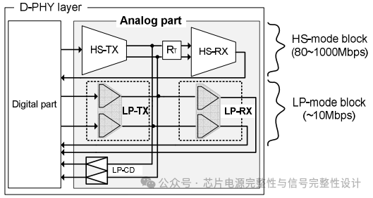 Figure 1. Schematic of the MIPI D-PHY Channel ModuleDesign and Simulation of MIPI D-PHYThe D-PHY digital module controls the transmission and reception of image data as well as control commands. The transmitter sends serialized data packets organized by the upper protocol layer. The receiver converts the received serialized data packets into parallel format. Figure 2 shows the signaling for each mode in MIPI D-PHY. The high-speed mode supports synchronous NRZ high-speed data transmission using SLVS technology. HS-TX transmits data using differential signals with a small swing (0.2Vpp) and a common-mode voltage of 0.2V. The bit rate for the signal pair ranges from 80Mbps to 1000Mbps. In high-speed mode, there are terminations at both ends of each transmission channel. The low-power function is primarily used for control and asynchronous LPDT (low-power data transmission). The single-ended low-power function has no termination and always appears in pairs. Due to the use of LVCMOS signaling, the low-power mode must support full swing data, such as 1.2V in the 10Mbps range. When no data is being transmitted, both the transmitter and receiver can be turned off to save power.
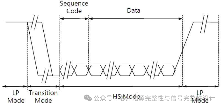 Figure 2. Signal Patterns for High-Speed Mode and Low-Power ModeFigure 3 shows the digital modules of the transmitter and receiver. The input signals from the upper protocol layer are on the left side of the transmitter. The output of TX and the input of RX are the analog interface modules.
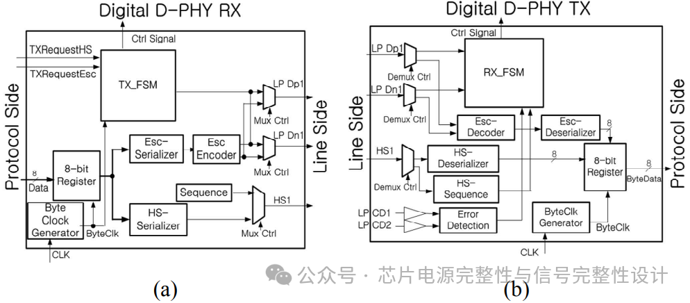 Figure 3. Block Diagram of Digital D-PHY. a) Transmitter, b) ReceiverFigure 4 shows the circuit diagram for the low-power mode. The CMOS driver is divided into three parts for synchronous switch output, noise reduction, and slew rate control. Figure 4(a) controls the slew rate and limits the output current by selecting an output buffer with a push-pull driver to maintain low EMI. This circuit has three inverter-type drivers, MND1+MPD1, MND2+MPD2, and MND3+MPD3, with different sizes and driving capabilities. As shown in Figure 4(b), the proposed precise LP-RX consists of two hysteresis comparators, an inverter, and a latch. The input voltages for high and low levels are Vref1 and Vref2.
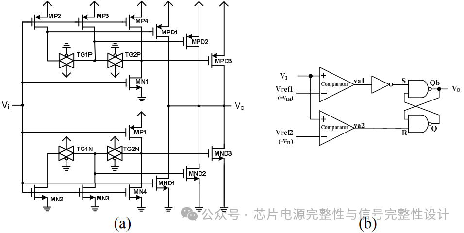 Figure 4. Circuit Diagram of Low-Power Mode. (a) LP-TX, (b) LP-RXIn Figure 5, HS-TX supports SLVS-based synchronous differential high-speed data transmission. SLVS is a chip-to-chip signaling protocol that uses differential voltage mode signaling. HS-TX transmits a differential voltage of 0.4Vpp, with a nominal single-line swing of 0.2Vpp and a common-mode voltage of 0.2V.
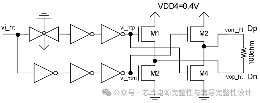 Figure 5. Circuit Diagram of HS-TXFigure 6 presents the HS-RX, which consists of termination resistors (ZID), a CMOS differential amplifier VCDA (very wide common-mode range differential amplifier), OTA, and a buffer stage. The first stage is VCDA, which suppresses fluctuations in ΔVCMRX and ΔVCD. The second stage is a single-ended OTA, which stabilizes the output of VCDA. The final stage is a buffer using multi-stage inverters to control the power consumption of the load capacitance.
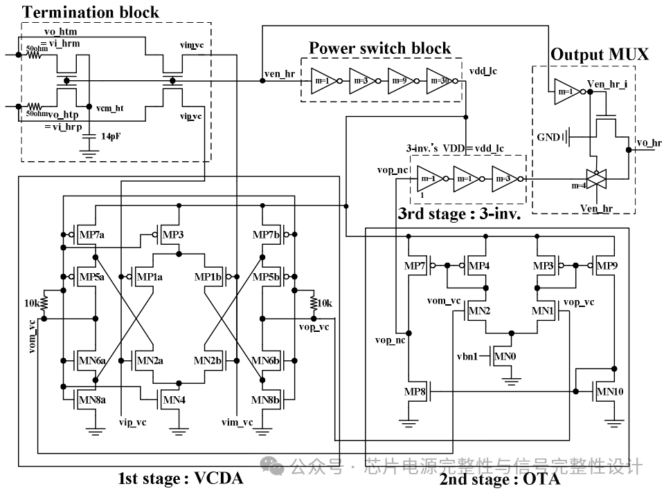 Figure 6. Circuit Diagram of HS-RXFigure 7 shows the simulation results of LP-TX under different load capacitances. The maximum current of LP-TX is limited by slew rate control, ensuring that the transition time of the LP-TX output meets specifications.
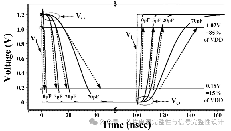 Figure 7. Simulation Results of LP-TX with Varying Load CapacitanceFigure 8 shows the measured eye diagram of the MIPI D-PHY chip with input 2^10-1 PRBS data. Figure 8(a) displays the eye diagram of the HS-TX differential output (VDp-VDn) at 200Mbps. The eye opening and width of HS-TX are 0.3Vpp and 3.5ns, respectively. Figure 8(b) shows the eye diagram of the HS-RX output at 100Mbps, with a jitter of 3.5ns.
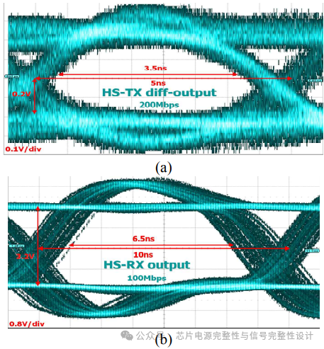 Figure 8. Measured Eye Diagram of MIPI D-PHY Chip (a) HS-TX, (b) HS-RXConclusionThe analog part of D-PHY consists of high-speed mode modules, low-power mode modules, and control modules, achieving data transmission speeds of 400Mbps and 500Mbps for TX and RX in high-speed mode, with power consumption of 0.52mW and 0.74mW, respectively, and a jitter of 5%.
Find Us
FIND US

Scan to Join the Community

Scan to Consult with the Teacher