Event: On June 11, 2025, Qualcomm announced the launch of the new Snapdragon AR1+ Gen 1 chip designed specifically for high-end smart glasses at the Augmented World Expo (AWE USA 2025) in the United States. Recently, the well-known domestic gold and jewelry company Laofengxiang announced its entry into the AI technology field with the release of its first AI glasses, which will be showcased at the Shanghai Old Expo from June 11 to 13.
According to global IT consulting firm Gartner, artificial intelligence technologies such as large language models are entering a maturity phase, and a large number of disruptive or highly impactful innovative technologies are expected to achieve mainstream adoption in the next two to five years.
According to Bain & Company’s “2024 Global High-Tech Industry Report,” the global AI hardware and software market is expected to continue growing at an annual rate of 40% to 55%, potentially reaching $780 billion to $990 billion by 2027.
Currently, China ranks second globally in terms of comprehensive AI capabilities, significantly ahead of other tiers, and continuous policy support is expected to catalyze the accelerated growth of the domestic AI application industry.
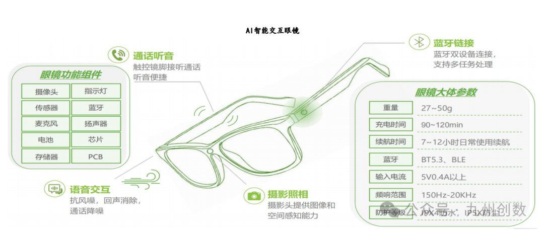
AI glasses are a new type of wearable device that integrates artificial intelligence technology with traditional glasses, capable of incorporating multiple devices or functions such as cameras, Bluetooth headsets, and AR (augmented reality). They can be categorized into non-display and display AI glasses based on whether they feature AR content display.
The unique advantage of AI glasses lies in their proximity to three key sensory organs: the mouth, ears, and eyes, allowing for natural and convenient input and output of sound, language, and visual information without the need for touch screens, thus freeing up hands while addressing the comfort shortcomings of XR devices.
Therefore, AI glasses will become one of the best carriers for deploying AI large models on mobile terminal hardware.
As AI+AR technology matures, penetration rates are expected to reach 70%, with sales reaching 1.4 billion units, comparable to smartphone shipment volumes. Among them, the BOM cost of SoC chips in AI camera glasses can account for up to one-third, and it is estimated that the market size for AI glasses SoC will exceed 10 billion yuan by 2030. Multi-modal interactive scenarios such as AI wearables and AI toys are gradually being realized, continuously raising performance requirements for SoC chips.
Rapid Penetration of AI at the Edge, Strong Growth in SoC Chips
SoC chips, short for System on Chip, are integrated circuits that combine multiple key components of a system onto a single chip, capable of achieving complete system functionality. SoC chips optimize size and power consumption by integrating software and interconnect structures designed for integration, enhancing system reliability, and significantly outperforming standard multi-chip systems in terms of efficiency. They are widely used in various electronic terminal devices for computation and control. SoC chips typically include one or more processor cores, memory, and various peripherals and interfaces for executing complex computation and control tasks:
1. Processor cores: including CPU, GPU, NPU, etc., for executing instructions, extreme processing, and controlling data flow.
2. Memory: including cache, RAM, and ROM for storing data and programs.
3. Peripheral interfaces: such as USB, Ethernet, HDMI, etc., for communication with other devices.
4. Power management unit: for power supply and power consumption management, achieving low-power operation and extending device battery life.
5. Other functional modules: such as audio processors, digital signal processors (DSP), etc., customized according to application needs.
SoC chips require high standards in research and development design, manufacturing processes, and hardware-software co-development technologies. Due to the increased integration of system-level chips, design must adopt reusable design concepts whenever possible. Therefore, most SoCs now use predefined IP cores (including soft cores, hard cores, and firm cores) to complete rapid design through reusable design methods. During the SoC design process, EDA tools connect self-designed or purchased IP cores, integrating various sub-functional modules within a single integrated development environment, reducing development redundancy costs and complexity, improving design efficiency, shortening chip time-to-market, and enhancing system scalability and compatibility.
NPU Integration to Meet Edge Computing Power Upgrade Needs
NPU (neural-network processing units) are embedded neural network processors specifically designed to accelerate neural network computations, employing a data-driven parallel computing architecture that excels at processing massive multimedia data such as video and images. Compared to traditional CPUs and GPUs, NPUs offer higher energy efficiency, lower latency, and stronger adaptability to various scenarios when handling AI tasks. TOPS quantifies NPU processing capability by measuring the number of operations (additions, multiplications, etc.) executed per second in trillions, while the true performance of an NPU results from the collaborative effects of memory bandwidth, software optimization, and system integration.
ISP Image and Video Module Collaboration Enhances Multi-modal Interaction Performance
ISP (Image Signal Processor) image signal sensors determine dynamic stabilization and low-power imaging capabilities. Under the same CMOS conditions, a high-performance ISP chip can improve image quality by 10% to 15%. AI glasses are evolving towards miniaturization, low power consumption, and high image quality, making multi-modal interaction capabilities crucial, with ISP cores being indispensable.
AI ISP is based on traditional ISP with the addition of AI post-processing algorithms through machine learning, i.e., the architecture of traditional ISP + NPU. Traditional ISP processes images using fixed algorithms and parameters, such as noise reduction, white balance, and exposure adjustment; AI ISP optimizes parameters adaptively through trained models to achieve smarter and more personalized image processing effects, better suited for applications requiring noise reduction, low light, and brightness enhancement. For example, Allwinner Technology has developed a new generation of AI-ISP noise reduction algorithms that consume 1T NPU computing power of the V851 chip, achieving 2-4 times sensitivity improvement under the same signal-to-noise ratio, enhancing image quality in low-light conditions.
According to MarketsandMarkets, the global SoC market is expected to reach approximately $206 billion by 2029, with a CAGR of about 8.3% from 2024 to 2029. The market shares of Asia and North America lead, with Asia accounting for 37% of the market size in 2023, and the SoC market in countries like China and India is expected to continue growing rapidly.
Global core SoC manufacturers include Qualcomm, MediaTek, Samsung, Apple, and Broadcom, with major downstream application areas including consumer electronics, smart driving, healthcare, AI computing, IoT, and industrial control. Domestic manufacturers are gradually penetrating from mid-to-low-end to high-end in the consumer electronics sector, accelerating domestic substitution in automotive electronics, and products in fields such as AIoT and industrial control are widely applied.
END