
The following questions are sourced from various inquisitive learners on Zhihu. As an advanced ceramics B2B platform serving the industry, CERADIR Advanced Ceramics Online strives to answer users’ queries. In the future, our editor will share related Q&A here weekly, and we welcome industry friends to ask us questions on Zhihu. If there are any omissions or errors, please feel free to criticize and correct us. Thank you!
 Now entering the Q&A mode
What is the difference between through holes and filled vias in ceramic circuit boards?

In the manufacturing of ceramic circuit boards (such as alumina Al₂O₃ and aluminum nitride AlN substrates), through holes (Through Hole Via, THV) and filled vias (Filled Via) are two key interconnection technologies:
(1) Through Holes: These are critical holes used to connect different circuit layers, including through holes (passing through the entire board), blind holes (from the outer layer to the inner layer), and buried holes (connecting between inner layers). They enable inter-layer signal transmission through copper foil, serving as channels for the copper foil lines to connect or conduct between conductive patterns across different layers of the circuit board.
The diameter tolerance of through holes must be controlled within ±10μm, and the diameter and position directly affect wiring density and signal integrity. They are suitable for high-frequency signal transmission (such as millimeter-wave radar requiring low-impedance paths) and high-density interconnections (such as HDI boards requiring stacked blind and buried holes).
Advantages: Simple process, low cost, suitable for low-density wiring.
Disadvantages: High-frequency signals are easily affected by the void effect (impedance discontinuity), and heat dissipation capability is limited.
(2) Filled Vias: This refers to the process of filling the interior of through holes with metal, aimed at ensuring conductivity within the through holes and preventing interference and loss during signal transmission.
The filling void ratio of filled vias must be less than 5%, and the quality of the filling directly affects the electrical performance and reliability of the circuit board. They are suitable for power module heat dissipation (copper-filled vias have a thermal conductivity >300W/mK) and cost-sensitive scenarios (the cost of oil-filled vias is 40% lower than that of electroplating).
Advantages: Superior high-frequency performance, doubled heat dissipation capability, and high structural strength (three times better resistance to thermal stress).
Disadvantages: Higher cost (30-50% more expensive than THV), complex process (requires control of filling void ratio <5%).
Q from @Ceramic Substrate PCB
What is a Silicon Carbide Mirror Blank?
Modern large optical telescope systems all adopt a reflective structure, with the core component being the mirror, akin to the “cornea” of a “thousand-mile eye.” The larger the diameter of the mirror, the stronger the telescope’s resolution and light-gathering ability.
Silicon carbide material is currently recognized as a high-performance mirror material in the international optics community.
The Changchun Institute of Optics, Fine Mechanics and Physics of the Chinese Academy of Sciences successfully developed a 4.03-meter diameter monolithic silicon carbide mirror blank in 2016. This mirror blank features a semi-closed lightweight structure on the back, achieving near-net-shape forming of ceramic materials, and is currently the largest publicly reported silicon carbide mirror blank in the world. Its application in telescopes or satellite imaging will significantly enhance resolution.
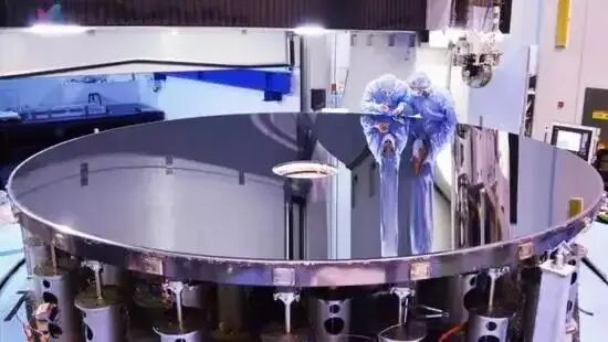
4.03 meters in diameter and weighing 1.6 tons, the silicon carbide SiC mirror
(Image source: internet, copyright belongs to the original author)
Q from @Set Sail for the Future
Welcome to follow our Zhihu organization account: CERADIR Advanced Ceramics Online
Search on Zhihu: ceradir
ABOUT CERADIR
“CERADIR™ Advanced Ceramics Online” – a vertical service platform for the advanced ceramics industry, dedicated to providing users with one-stop B2B solutions, professionally serving the upstream and downstream factories, traders, and service providers of the global advanced ceramics supply chain, and attracting global suppliers and buyers to settle in.
 Share
Share Like
Like View
View