1About Bit-Banding Operations
Bit-banding, abbreviated as bit-band, is also known as bit-segment. After supporting bit-banding operations, you can use ordinary load/store instructions to read and write individual bits.
Many friends come from learning the 51 microcontroller and know that the P1.1 pin can be controlled individually; the pin we are operating on is a Bit bit.
We all know that in STM32, you cannot directly operate on a specific Bit of a register, for example, to control the ODR1 in the data output register of the PA port individually, as shown below:

The STM32F1 core Cortex-M3 has long considered this issue. To achieve direct operation on ODR1 like this Bit, a dedicated address area (bit-band alias) was opened up in the core: You can map Bit positions like ODR1 (bit-band area) to the corresponding address in the bit-band alias area, and by operating on the mapped address, you can operate on the ODR1 bit.
In simple terms, this is a mapping operation, but there are many conventions to follow for this mapping operation.
2Mapping Relationships in Bit-Banding Operations
In Cortex-M3, there are two areas that implement bit-banding operations, one is the SRAM area of the lowest 1MB range, and the second is the on-chip peripheral area of the lowest 1MB range.
These two areas are marked in red in the following figure:

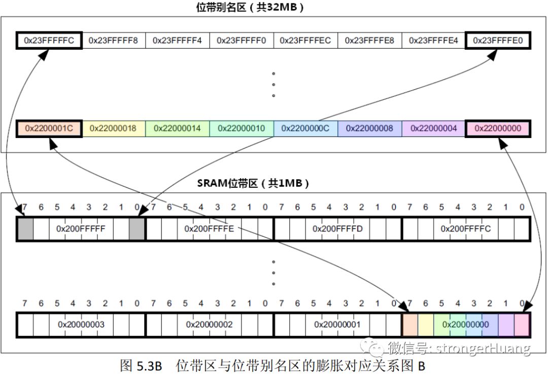
These two 1MB will be mapped to another two address areas:

3Bit-band Area to Alias Area Calculation Formula
The main purpose of bit-banding operations: to calculate the alias area address (AliasAddr) from the bit address (A).
1. SRAM Area Calculation Formula
AliasAddr=0x22000000+((A‐0x20000000)*8+n)*4=0x22000000+(A-0x20000000)*32+n*4
2. On-chip Peripheral Area Calculation Formula
AliasAddr=0x42000000+((A-0x40000000)*8+n)*4=0x42000000+(A-0x40000000)*32+n*4
Since the mapping relationship is the same, the principle of the formula is also the same; only the addresses are different. The calculation formula needs to be understood in conjunction with the bit expansion correspondence shown in the above figure.
*8: 1 word is 4 bytes
*4: 1 byte is 8 bits
4Code Implementation
#define BITBAND_RAM(RAM, BIT) (*((uint32_t volatile*)(0x22000000u + (((uint32_t)&(RAM) - (uint32_t)0x20000000u)<<5) + (((uint32_t)(BIT))<<2))))#define BITBAND_REG(REG, BIT) (*((uint32_t volatile*)(0x42000000u + (((uint32_t)&(REG) - (uint32_t)0x40000000u)<<5) + (((uint32_t)(BIT))<<2))))
A. Write 0 to Bit1 of RAM address 0x20001000
BITBAND_RAM(*(uint32_t *)0x20001000, 1) = 0;uint8_t Val;Val=BITBAND_RAM(*(uint32_t *)0x20001000, 1);BITBAND_REG(GPIOA->ODR, 1) = 1;uint8_t Val;Val=BITBAND_REG(GPIOA->ODR, 1);Here, we are operating on a specific address, similar to operating on a pointer.
5Advantages and Disadvantages of Bit-Banding Operations
6Conclusion
For more details about the bit-banding operations of Cortex-M3, please refer to the Cortex-M3 Technical Reference Manual (Authoritative Guide).
Later Cortex-M processors no longer support bit-banding operations; from the perspective of compatibility with future software, it is not very recommended for everyone to continue using it.
However, bit-banding operations are a classic; here I share it for everyone to understand, and I hope it helps you.

END
Source: Embedded Column
→ Follow to avoid getting lost ←