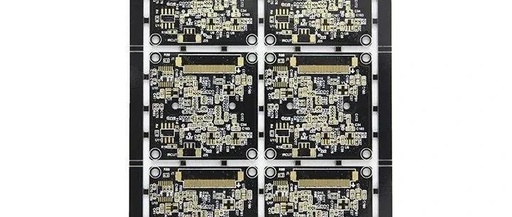
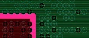
Quality Killers in PCB Manufacturing – Photoresist Semi-Polymer
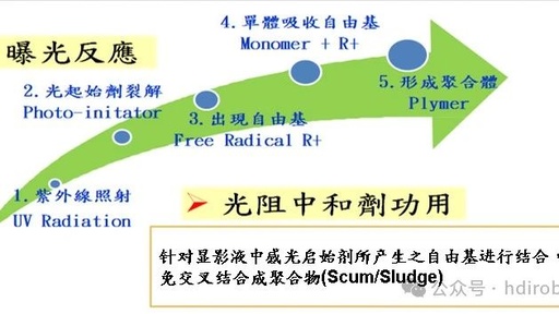
Quality Killers in PCB Manufacturing – Photoresist Semi-Polymer In the PCB manufacturing process, many tasks require the use of “photoresist materials,” including inner layer wet film, inner layer dry film, outer layer dry film, and green solder mask. It is a chemical material that, after exposure to light, produces different solubility in the developing solution … Read more