
Design of Mark Points in PCB Production
1. A mark point corresponding to the whole board must be located on the diagonal of the PCB’s long edge. For chips with an integrated circuit pin center distance of less than 0.65mm, there must be a corresponding mark point on the diagonal of the integrated circuit’s long edge. When there are surface-mounted components on both sides of the PCB, mark points should be added according to this rule on both sides.
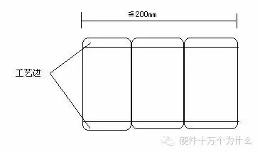
2. A 5mm process margin must be left on the edge of the PCB (minimum distance requirement for machine clamping), and it must be ensured that chips with an integrated circuit pin center distance of less than 0.65mm are more than 13mm (including the process margin) from the edge of the board; the four corners of the board should have a Ф5 round corner. The PCB should be made using a panel method. Considering the current degree of PCB curling, the best splicing length is about 200mm (equipment processing dimensions: maximum length of 330mm; maximum width of 250mm). In the width direction, splicing should be avoided as much as possible to prevent bending during production. See the figure below:
3. Functions and Categories of Mark Points
Mark points, also known as reference points, provide common measurable points for all steps in the assembly process, ensuring that each device used in assembly can accurately position the circuit pattern. Therefore, mark points are crucial for SMT production.
4. Recommended Mark Point Design Specifications by Our Department
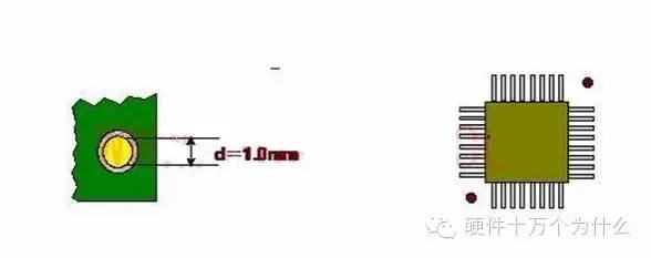
1) Shape: It is recommended that the mark point be marked as a solid circle with a diameter of R=1.0mm;
2) A complete mark point consists of a marking point (or feature point) and a clear area.

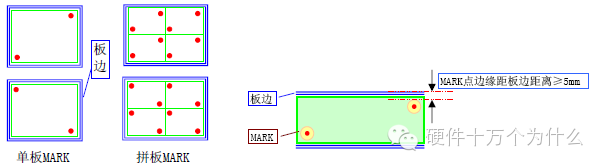
3) Location: Mark points should be located at opposite positions on the diagonal of the single board or panel and as far apart as possible; it is best to distribute them at the longest diagonal positions (as shown in the mark point position diagram).
4) To ensure the accuracy requirements for mounting, SMT requires that there must be at least one pair of mark points that meet the design requirements and can be recognized by SMT machines in each PCB, and there must also be a single board mark (when using a panel), while panel marks or combination marks only serve as auxiliary positioning.
5) When using a panel, the relative positions of the mark points on each single board must be the same. For any reason, the position of the mark point on any single board in the panel should not be moved, which would cause asymmetry in the positions of the mark points on each single board;
6) All mark points on the PCB are only valid if they appear in pairs and are located on the same diagonal. Therefore, mark points must appear in pairs to be usable (as shown in the mark point position diagram).
7) The distance from the edge of the PCB to the edge of the mark point (clear area) must be ≥5.0mm (minimum distance requirement for machine clamping) (as shown in the mark point position diagram).
(Mark Point Position Diagram)
8) Dimensions
A. The minimum diameter of the mark point marking is 1.0mm, and the maximum diameter is 3.0mm. The size variation of mark point markings on the same printed circuit board cannot exceed 25 microns;
B. It is particularly emphasized that all mark points on the same board number PCB must be consistent in size (including PCBs of the same board number produced by different manufacturers);
C. It is recommended that all mark point marking diameters be uniformly set to 1.0mm.
9) Clear Area Requirements
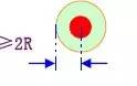
Around the mark point marking, there must be a clear area without other circuit features or markings. The radius of the clear area r≥2R, where R is the radius of the mark point; when r reaches 3R, the machine recognition effect is better.
10) Materials
Mark point markings can be bare copper or bare copper protected by a clear anti-oxidation coating. If solder mask is used, it should not cover the mark point or its clear area.
11) The brightness of the mark point should remain consistent.
12) Flatness: The surface flatness of the mark point marking should be within 15 microns.
13) Contrast
A. The best recognition performance can be achieved when there is high contrast between the mark point marking and the substrate material of the printed circuit board.
B. The inner background of all mark points must be the same.
Below are experiences shared by others in this area for reference
Classification of Mark Points:
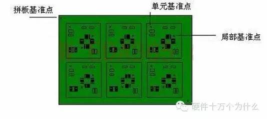
1) Mark points are used for optical positioning during solder paste printing and component placement. Based on the function of mark points on the PCB, they can be divided into panel mark points, single board mark points, and local mark points (also known as device-level mark points).
2) There should be at least three mark points on the process edge of the panel and on the single board that does not require splicing, arranged in an L shape, with diagonal mark points being asymmetrical about the center.
3) If both sides have mounted components, there should be mark points on each side.
4) For single boards that need splicing, mark points should be placed as much as possible; if there is no position for placing mark points, they can be omitted on the single board.
5) For devices such as QFP with a lead center distance of ≤0.5mm and BGA with a center distance of ≤0.8mm, local mark points should be set near the diagonal of the center point of the device for precise positioning.
6) If several SOP devices are relatively close (≤100mm) forming an array, they can be regarded as a whole, and two local mark points should be designed at their diagonal positions.
Design Description and Size Requirements:
1) The shape of the mark point is a solid circle with a diameter of 1mm, made of copper, surface tin-plated, and care should be taken regarding flatness, smooth and neat edges, and a color that is significantly different from the surrounding background color; the solder mask opening should be concentric with the mark point, with diameters of 3mm for panels and single boards, and 1mm for local mark points.
2) For mark points on a single board, the center distance to the edge of the board should not be less than 5mm; for mark points on the process edge, the center distance to the edge of the board should not be less than 3mm.
3) To ensure the recognition effect of printing and placement, there should be no pads, vias, test points, traces, or silkscreen markings within the range of the mark point, and it should not be cut by V-CUT grooves that would prevent machine recognition.
4) To increase the contrast between the mark point and the substrate, copper foil can be laid under the mark point. The inner background of mark points on the same board should be the same, i.e., whether there is copper foil under the mark point should be consistent.
5) Mark points for single boards and panels should be designed as components, while local mark points should be designed as part of the component package to facilitate accurate coordinate values for positioning.
Optical Reference Points in PCB Design!
On PCB boards with surface-mounted components, to locate the entire PCB, it is usually necessary to place optical reference points at the four corners of the PCB, generally three are sufficient. The common reference points mainly include three types: panel reference points, unit reference points, and local reference points.
Structure of Reference Points
(1) Panel Reference Points and Unit Reference Points
Shape/Size: A solid circle with a diameter of 40mil. Solder mask opening: a circle concentric with the reference point, with a size twice the diameter of the reference point. At the edge of 2mm diameter, a circular or octagonal copper wire is required as a protective ring. The inner background of optical positioning reference symbols on the same board must be the same, i.e., whether there is copper foil under the three reference symbols should be consistent.
 (2) Local Reference Points
For devices such as QFP with a spacing ≤0.4mm and BGA, CSP, FC with a spacing ≤0.8mm, local reference points need to be placed.
Size/Shape: A solid circle with a diameter of 40mil.
Solder mask opening: treated according to normal pads, and the outer copper ring can be omitted.
Placement of Reference Points:
General Principle:
Single boards processed by SMT equipment must have reference points. The number of reference points on one side must be ≥3.
When laying out a single side, reference points should only be placed on the component side. In a double-sided layout, reference points should be placed on both sides. For double-sided reference points, except for mirrored panels, the positions of the reference points on both sides must be basically consistent. See the figure below.

(1) Placement of Panel Reference Points
Panels need to place panel reference points and unit reference points.
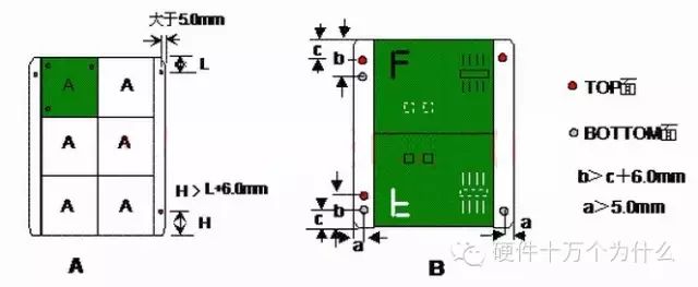
The number of panel reference points and unit reference points should each be three. They should be distributed in an L shape at the edge of the board and as far apart as possible. The position requirements of panel reference points are shown in the figure below A.
When using mirror symmetry for panel placement, the reference points on the auxiliary edge must meet the requirement of overlapping after flipping, see the figure below B.
 (2) Placement of Unit Board Reference Points
The number of reference points is three, distributed in an L shape at the edge of the board, with the distance between each reference point as far apart as possible. The distance from the reference points to the edge of the board must be greater than 5mm. If it cannot be guaranteed that all four edges meet this requirement, at least the transmission edge must meet the requirement.
【1】Interest Driven Passion
【2】Should Hardware Engineers Draw PCBs Themselves?
【3】How Long Should PCB Traces Be??
【4】How Wide Should PCB Traces Be?
【5】Inner Layers of PCB
【6】Vias
【7】Can PCB Traces Have Sharp Angles and Right Angles?
Is it Necessary to Keep Dead Copper? (PCB Islands)
【9】Can Vias Be Placed on Pads??
PCB Materials, What Exactly Does FR4 Refer To?
Why is the Solder Mask Layer Usually Green?
Steel Mesh
Pre-layout
Key Points of PCB Layout and Wiring
Cross Segmentation Traces
Signal Reflection
Dirty Signal
Surface Treatment Processes Such as Gold Plating, Tin Plating, etc.
Trace Spacing
Positioning of Capacitors
Crosstalk
PCB Flying Needle Testing
Overview and Simulation of FPC
Why Do PCBs Deform and Bend? How to Solve It?
Understanding “Characteristic Impedance” in One Article
Layer Design of PCB
Reflow Paths for High-Speed Circuit PCBs
Power Handling and Plane Segmentation in PCB Design
Zigzag PCB Traces – Tabbed Routing
What is the Dielectric Loss Angle of PCB?
How Does Copper Foil Roughness Affect High-Speed Signals?
Why Can’t Crystals Be Placed at the Edge of the PCB?
What is a High-Speed Signal?
What is a Transmission Line?
Pre-emphasis, De-emphasis, and Equalization
How to Utilize PCB Heat Dissipation
“Stub” in PCB Design
Debate: Should There Be Ground Protection Traces Between Traces or Not?
PCB Copper Pour
Rules to Follow When Designing PCBs
“Fake Eight Layers” in PCB Layer Design
In addition to Stripline and Microstrip, There is Also “Co-planar Waveguide”
Parameters Related to PCB Pad Design Process
Why Should Ground Holes Be Drilled on PCB Edges?
PCBs That Are Easier to Heat Dissipate: Aluminum Substrates
Why Should Reference Planes Be Hollowed Out?
Crystal Oscillator PCB Design
PCB Design of DC/DC Power Supply with EMC Considerations
PCB Turns, Round Traces Are Not Always the Best
Why Should Vias Be Sealed? (Conductive Via Plugging Process)
Key Points for Power PCB Layout and Wiring
Published Books by Hard Ten


“DCDC Power Supply Volume” is currently in the publishing process, expected to be on sale in May, stay tuned.