Why SoC Performance Depends on Architecture and Process?
Click the above PC Enthusiasts to follow us
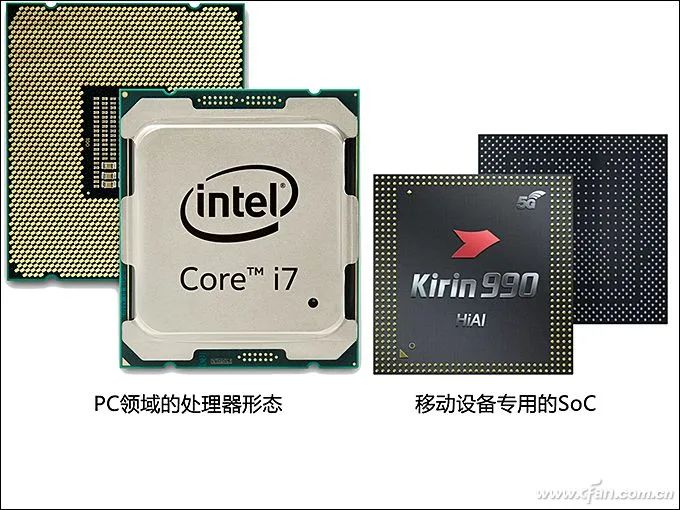
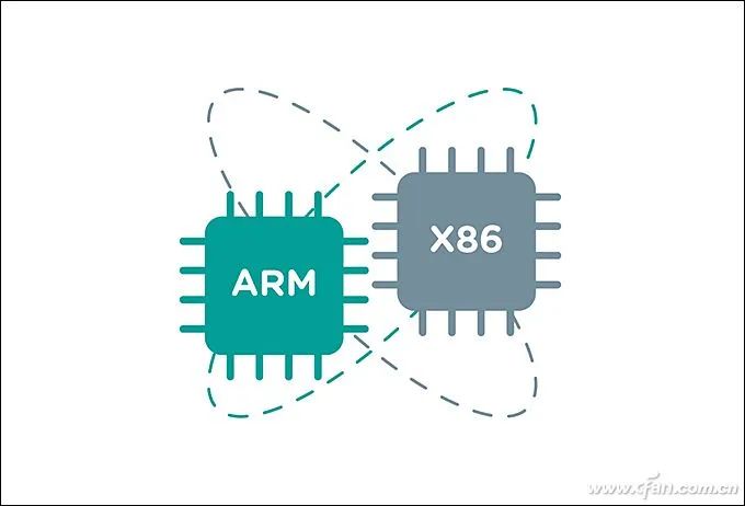
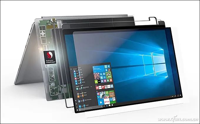
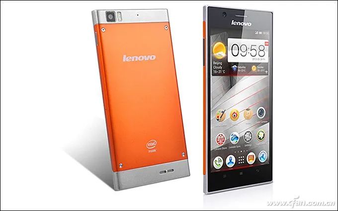
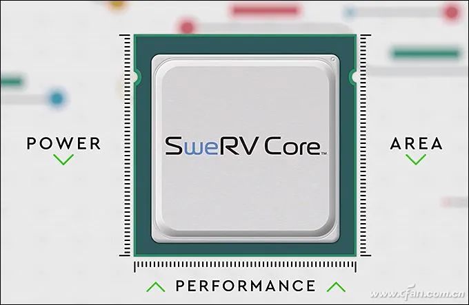
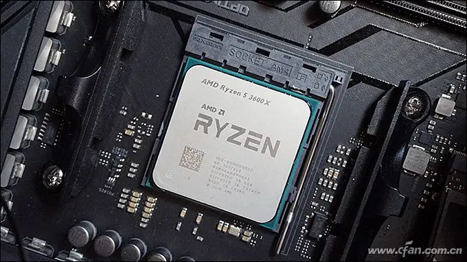
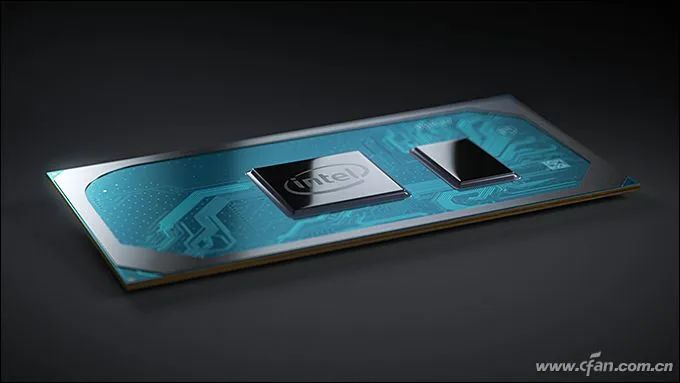
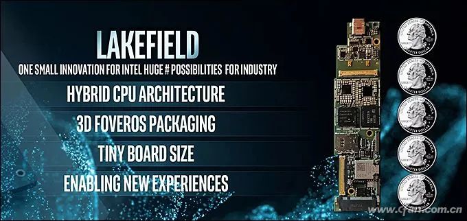
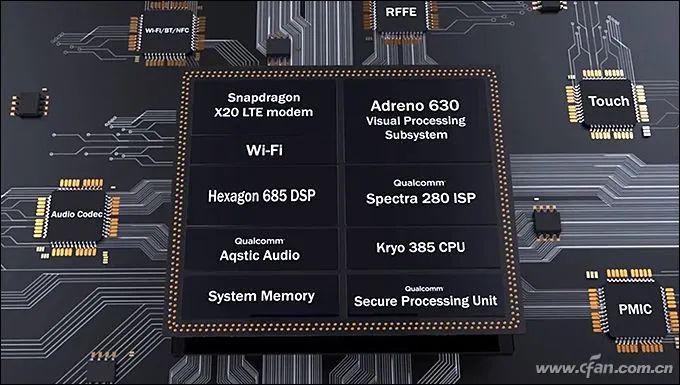
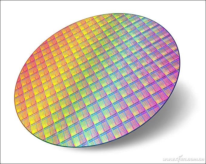
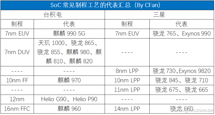
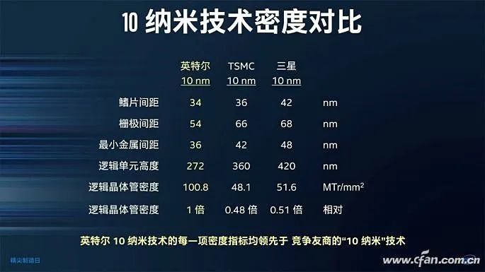
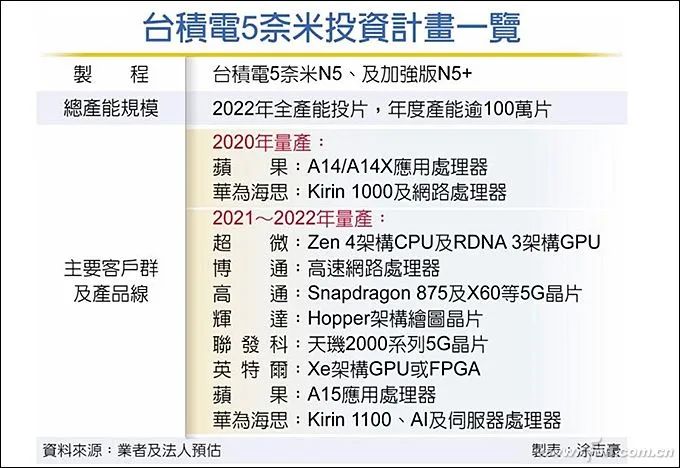
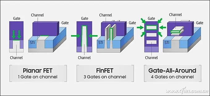
The “heart” of PCs (including desktops, laptops, all-in-ones, and 2-in-1 devices) and mobile devices (smartphones, tablets running Android and iOS) is a chip, but they have fundamentally different characteristics, leading to divergent development paths for these two types of computing devices.This image is for reference only; the size of mobile chips is much smaller than that of PC chips.The innate attributes of architecture and instruction setsAlthough mobile phones are becoming increasingly powerful, we still cannot expect them to replace PCs; in 3D gaming and many professional design fields, the performance of the two remains vastly different.The reason lies in the fact that the “hearts” of these two types of computing devices adopt different architectures and instruction sets, each with its own “inherent flaws”.ARM and X86 architecturesFirst, we need to know that mobile processors are almost all based on the “ARM architecture”, while PC processors are predominantly based on the “X86 architecture”.However, in certain fields and under special circumstances, ARM and X86 have shown “cross-border” behavior. For example, Intel has previously launched mobile-specific X86 architecture processors (such as Atom Z2580), and now many energy-efficient servers have also switched to ARM architecture processors.RISC and CISC instruction setsARM architecture processors originate from “RISC” (Reduced Instruction Set Computer), which is best optimized for commonly used commands, providing a simpler and more efficient execution environment, while less frequently used functions are completed through various simplified instruction combinations.RISC delegates complexity to the compiler, sacrificing program size and instruction bandwidth in exchange for a simpler and lower-power hardware implementation.X86 architecture processors originate from “CISC” (Complex Instruction Set Computer), which is suitable for more complex application environments. CISC increases the complexity of the processor itself at the cost of power consumption to achieve higher performance.However, X86 architecture can improve the execution efficiency of specific tasks and reduce power consumption through support for new instruction sets (such as SSE4.1, AVX-512, etc.).In other words, RISC has the innate advantages of high efficiency and low power consumption, perfectly matching computing devices like smartphones and tablets that prioritize energy efficiency. While using RISC in PCs may extend battery life, it significantly compromises performance, compatibility, and efficiency in running professional software.The reputation of Windows devices powered by ARM architecture Snapdragon mobile platforms is not ideal.CISC, while having high performance, also has a fundamental drawback of high power consumption, making it difficult for small devices like smartphones to manage heat and power consumption.The Lenovo K900 phone powered by the X86 architecture Atom Z2580 chip also suffers from poor compatibility, heat, and battery life.If you want to learn more about RISC and CISC instruction sets, please refer to the article “A12X and Snapdragon 855 So Strong, Can ARM Really Replace X86?”“.RISC-V architecture makes a strong entryTo break the monopoly of X86 architecture and the high licensing fees of ARM architecture, a new instruction set architecture called “RISC-V” has emerged based on the RISC instruction set.Compared to its relative “ARM” architecture, RISC-V’s biggest feature is that it is free and open; it can be used freely for any purpose, and anyone can design, manufacture, and sell RISC-V-based chips or software.This openness marks a complete first in the processor field.Unfortunately, the RISC-V architecture ecosystem is still under construction and improvement. Currently, it is mainly used in embedded chip fields, with giants like Western Digital, Qualcomm, NVIDIA, Alibaba, and Samsung already joining the RISC-V architecture for various applications such as hard drive controllers, GPU memory controllers, mobile SoCs, AI accelerators, and 5G RF front-end modules for millimeter-wave RF processing.Western Digital has developed the SweRV processor based on the RISC-V instruction set with a proprietary general-purpose architecture.Reports suggest that with the current development speed of RISC-V, there is a chance to compete with ARM for customers of mobile processors like Qualcomm, Apple, Samsung, and MediaTek by 2022, and it is expected to enter the server market by 2025.Not all processors are SoCsBoth home PCs and smartphones have only one “heart”, but in the former, this chip is referred to as the “processor”, whereas in the latter, it is always emphasized that this is a “SoC”.So, what is the difference between a processor and a SoC?Processors in the PC fieldIn the PC field, chips like Core i5-9400F and Ryzen 5-3600 are purely “CPUs” (Central Processing Units) because they only integrate a single CPU core on the PCB substrate.However, in the low-power domain represented by laptops, processors are gradually transitioning to SoCs, integrating CPU, GPU, memory controllers, and PCIe controllers into a single chip or board.10th generation Core processors integrated with CPU/GPU and chipset.CFan previously introduced Intel’s latest Lakefield processor, built using Foveros 3D packaging technology, which integrates a large Sunny Cove architecture CPU core, four Tremont architecture small core CPUs, and Gen 11 GPU within the size of a coin, while also consolidating different IP units.In other words, Lakefield perfectly realizes the transformation of X86 architecture chips from processors to SoCs, meaning that some laptops (including 2-in-1 devices) will no longer be equipped with pure CPUs.SoCs in mobile platformsThe integration level of each mobile “heart” is no less than that of Lakefield, so the processor chips in mobile phones are all complete SoCs (System on Chip), containing CPU, GPU, Image Signal Processor (ISP), Digital Signal Processor (DSP), Neural Processing Unit (NPU), Modem, and other functional modules within a single chip.The single-chip design of SoCs maximizes motherboard layout efficiency, helps slim down devices, enhances communication speed between various IP units, and significantly reduces overall power consumption.Process technology determines combat powerSimilar to processors in the PC field, SoCs designed for smartphones are also cut from a whole wafer, and their performance potential is closely related to process technology.The more advanced the process technology selected for an SoC, the higher the potential for unlocking higher clock speeds, lower heat generation, lower power consumption, and better stability.Process iteration and updatesThe unit of process technology is “nm” (nanometers); “theoretically”, the smaller the number, the more advanced it is. For example, 7nm is stronger than 8nm, and 12nm is superior to 16nm.Currently, except for a few chips like MediaTek Helio P65, P90, and G90, most of the latest SoCs have crossed the 10nm process threshold, showing significant improvements in overall energy efficiency compared to their 14nm and 16nm predecessors.Secrets behind process numbersWhether it’s Intel, TSMC, Samsung, or GlobalFoundries, different wafer foundries have their own customized standards for process technology. The same process may have significant differences in metrics like fin pitch, gate pitch, minimum metal pitch, logic cell height, and logic transistor density.For instance, Intel’s 14nm process is more advanced than Samsung and TSMC’s 10nm in the aforementioned metrics, and TSMC’s 16nm reputation was better than Samsung’s 14nm at that time.In addition to major version upgrades like 10nm to 7nm, process technology also undergoes small innovations periodically.For example, TSMC’s 16nm process has derived the first generation FinFET (16nm FF), second generation FinFET Plus (16nm FF+), and third generation 16nm FinFET Compact (16nm FFC), while Samsung prefers to distinguish first generation Low Power Early (LPE), second generation Low Power Plus (LPP), third generation Low Power Compact (LPC), and fourth generation Low Power Ultimate (LPU).If you want to learn about the impact of EUV lithography on process performance, please refer to the article ““Hope Comes from New Processes! What Are EUV and GAAFET Technologies?”“.Expectations from the futureAfter launching the 7nm+EUV process, TSMC’s latest 6nm and 5nm process technologies are also ready for mass production. The former is a transitional performance process that everyone can understand, while the latter is the most important process node in the next 1-2 years, and TSMC will further subdivide it into 5nm (N5) and 5nm+ (N5+).This year, there will be mass production of chips based on the 5nm process, such as Apple’s A14/A14X, Huawei Kirin 1000, and network processors.In 2021, Apple A15, Huawei Kirin 1100, AMD Zen 4/RDNA3, Snapdragon 875+X60 5G baseband, and MediaTek Dimensity 2000 will also join the ranks. It is reported that compared to the first generation 7nm DUV, the new 5nm chip based on Cortex A72 cores can provide 1.8 times the logic density, a 15% speed increase, or a 30% reduction in power consumption, with SRAM of the same process also being excellent and area-reduced.After mass production of Samsung’s 10nm LPP process, they skipped the first generation 7nm DUV and directly started the latest 7nm+EUV process. After 2020, Samsung will successively introduce 6nm LPP, 5nm LPE, and 4nm LPE, and will begin to introduce Gate-All-Around Field Effect Transistors (GAAFET) at the 3nm node to replace the existing FinFET technology.After a while, ARM will officially release the next generation flagship CPU core Cortex-A78 based on a custom RISC architecture, as well as the next generation GPU core Mali-G78. When combined with 5nm technology, they will bring unprecedented overall performance improvements. The Kirin 1000 series is expected to be the first SoC to incorporate these elements and is anticipated to be launched in September, with mass production in October alongside the Mate 40 series.At that time, through benchmarking the Kirin 1000 against existing flagship SoCs like Snapdragon 865, we will gain a more intuitive understanding of the performance foundation of the next generation of SoCs.After reading this article, you may also click: