(Source: allaboutcircuits)Understand how Application-Specific Integrated Circuits (ASICs) help companies leverage their critical IP and differentiate themselves from competitors using off-the-shelf ICs.Off-the-shelf integrated circuits (ICs) offer numerous advantages to electronic system designers. The most notable advantage is convenience. Vendors provide evaluation boards and other support, enabling designers to easily prototype solutions and bring them to market. However, this convenience comes at a cost: it makes differentiation on critical metrics for customers, such as power efficiency, functionality, and size, more challenging.Evaluation boards based on off-the-shelf ICs provide a potential quick path to mass production. However, solutions based on these off-the-shelf products inevitably have converging feature sets. System designers have limited opportunities to optimize for specific sensors and displays, application computational requirements, or power conversion strategies best suited for the target use case.These limitations are becoming increasingly apparent. Users today want to leverage technologies like machine learning and deploy ultra-low-power systems that only require a single battery charge over their lifetime. General-purpose ICs mean these users must contend with fixed performance ranges and operating modes, with only minor changes to electrical characteristics possible through firmware modifications or external mixed-signal circuits. These external circuits also add to the total cost of producing hardware.Custom ASICs: Unlocking DifferentiationCustom Application-Specific Integrated Circuits (ASICs) can avoid the pitfalls of using off-the-shelf silicon throughout the system design. With custom hardware, designers can optimize the system more comprehensively.For example, hardware accelerators tailored for machine vision algorithms can significantly increase data throughput while reducing power consumption. This is because hardware acceleration can replace many software instructions. By saving on the data movement required between memory and registers for algorithms based on general-purpose microprocessors, throughput can be significantly enhanced at lower power consumption.With ASICs, application developers can provide practical insights to hardware design teams, further enhancing functionality. For instance, information can be provided on how to optimally cut power to individual units when not in use. In many cases, although general-purpose ICs have broad power gating support, the algorithms controlling when units enter ultra-low-power states must be applied judiciously to ensure that sleep modes do not affect functionality.In addition to enhancing the ability to tailor hardware for applications, custom silicon also sets up a strong barrier against piracy. Because the bill of materials (BOM) relies on standard ICs, competitors can easily determine how the system is assembled. Even if the processor in the solution supports code encryption, many features provided by the IC vendor are part of their software development kits, making reverse engineering the system not necessarily a significant obstacle.Recovering the netlist from an ASIC requires more extensive analysis and the ability to peel back the device layer by layer. Even so, a counterfeiter would still need sufficient resources to understand the relationship between the netlist and system functionality. They would also need access to their own custom IC design resources to replicate it.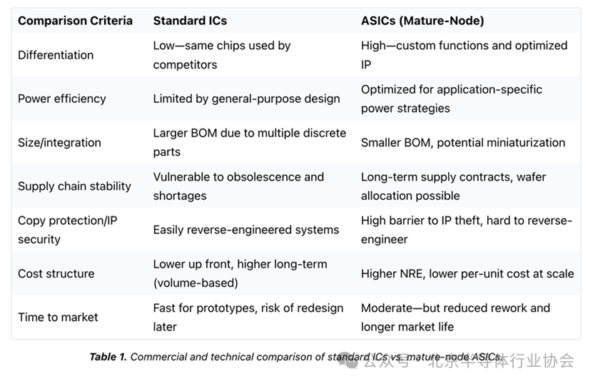 Mature Node ASICs: Zero-Cost CustomizationASICs do not need to include all or even most design features. Typically, by adding strategically important features, custom silicon can gain significant advantages over mass-market ICs. Among other benefits, this targeted design helps reduce manufacturing complexity and BOM size.For example, a design uses a catalog BLE IC paired with a custom 130 nm ASIC for analog and power management. To ensure long-term flexibility, the ASIC specifies dual interfaces (e.g., I2C, SPI, GPIO, and power management modules) to be compatible with BLE ICs from multiple vendors. This meets the needs for analog BLE, Arm cores, and flash memory without incurring the high costs of full integration on advanced nodes.Companies often cleverly leverage ASIC-based improvements by focusing on the sensor interface or power conversion circuits of the system. In many cases, this allows them to consolidate multiple discrete components into a single part. Integrating analog signal conditioning, digital signal processing, and communication interfaces into a single ASIC can miniaturize sensor devices to fit into tight spaces. Custom switching mode strategies for specific motors can enable drones to fly longer on a single charge.This approach does not require adopting more expensive, cutting-edge process technologies like those used by multi-core processors and other advanced digital device vendors. Devices such as IoT, industrial controllers, and automotive control subsystems require higher voltage and analog integration, which far exceed the raw gate counts that cutting-edge processes can provide.Mature CMOS nodes like 180 nm and 130 nm are sufficient to meet the performance needs of target coprocessors and can directly support the voltages required by many sensors and power control devices. ICs manufactured using the latest processes below 10 nm are inefficient in supporting analog circuits and are significantly more expensive. A typical 180 nm mask set can easily cost around $50,000, while cutting-edge processes can cost millions.A comprehensive design suite includes proven memory, IO, and standard digital logic function IP libraries. Additionally, we provide a rich array of foundry or third-party IP for analog front ends and communication interfaces, further reducing design risks and shortening time to market. Mature nodes offer robust yields and easy-to-understand design rules, combining custom advantages, low-risk characteristics, and cost structures to support a wide range of applications.From Customization to Competitive AdvantageIn an era where widely used commercial silicon erodes profits and weakens brand uniqueness, mature node ASICs provide a transformative lever. Because custom ASICs do not require an “all or nothing” approach to system architecture, users can focus on leveraging their most critical intellectual property and differentiating in ways that competitors using off-the-shelf devices cannot achieve.Given the advantages of the ASIC approach, we should ask ourselves the following questions:
- If you had a chip, what unique features could your next-generation device offer?
- How much risk and cost could you eliminate from your supply chain by integrating discrete components into a single ASIC?