


Chip manufacturing’s “final step”:
Unveiling the mysterious “tape-out” and its high costs

In the world of chips (integrated circuits), there is a crucial step that determines whether the hard work of countless engineers can be transformed from blueprints into reality, and that is—”tape-out”. What does this industrial-sounding term really mean? Why is it often said in the industry that “one tape-out can lead to bankruptcy”? Today, we will unveil its mysterious veil.
01
What is tape-out?
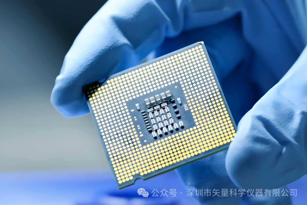
In simple terms, tape-out is a small batch trial production after the chip design is completed. You can think of it as:
-
The final inspection station for design: After designers complete the design and simulation verification, they hand over the final layout design files (such as GDSII) to the chip foundry (Fab).
-
Small batch sample manufacturing: The foundry uses this set of design files to produce a small batch of chip samples (usually ranging from dozens to hundreds).
-
The touchstone for functionality and performance: This batch of samples will be returned for strict testing to verify whether the production process is feasible and whether the actual performance and functionality of the chip meet the design requirements.
The success or failure of tape-out is a key node that determines whether the chip can enter mass production. Only after the tape-out samples pass testing can large-scale production confidently commence.
02
Why is tape-out so expensive?
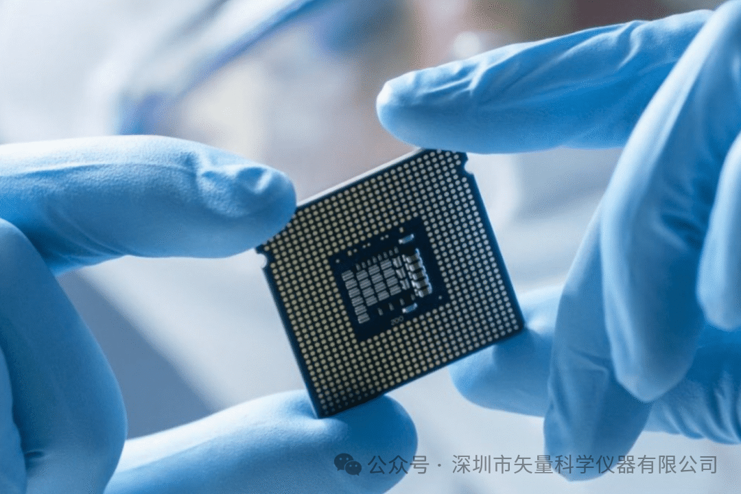
The cost of tape-out does not have a unified answer; it is greatly influenced by factors such as the process technology (e.g., 40nm, 14nm, 7nm), the complexity of chip design, and the scale of production. However, its high cost is enough to intimidate startups!
The root of the high cost of tape-out lies in:
-
Sky-high “molds” – Masks: This is the largest cost item! Masks are the core of the photolithography process, and the design patterns need to be accurately transferred to the wafer through them.
-
The more advanced the manufacturing process (the smaller the node), the more mask layers are required:For example, the 28nm process requires about 40 layers, 14nm about 60 layers, and 7nm may require 80 layers or even more. Each layer of mask is a significant expense. A full set of masks for advanced processes (such as 7nm/5nm) can cost millions or even tens of millions of dollars! This is almost the largest part of the tape-out cost.
-
Complex foundry fees: Chip manufacturing itself involves hundreds or even thousands of precise processes (photolithography, etching, doping, deposition, polishing, etc.). Each step requires expensive equipment, a clean environment (clean rooms), and extremely high process control precision, all of which contribute to high operating costs.
-
Depreciation costs of expensive equipment: Semi-conductor manufacturing equipment (such as photolithography machines, etchers, etc.) can cost tens of millions or even hundreds of millions of dollars each. The huge purchase and maintenance costs of this equipment are allocated to each tape-out production.
-
The cost of “small scale” – Lack of economies of scale: Tape-out is essentially a very small batch production. The high costs of masks and equipment depreciation, among other fixed costs, can only be shared by this small number of chips, leading to extremely high costs per chip. In contrast, during mass production, although wafer costs are the main part, the cost per chip is significantly reduced due to the large output.
03
How long does tape-out take?
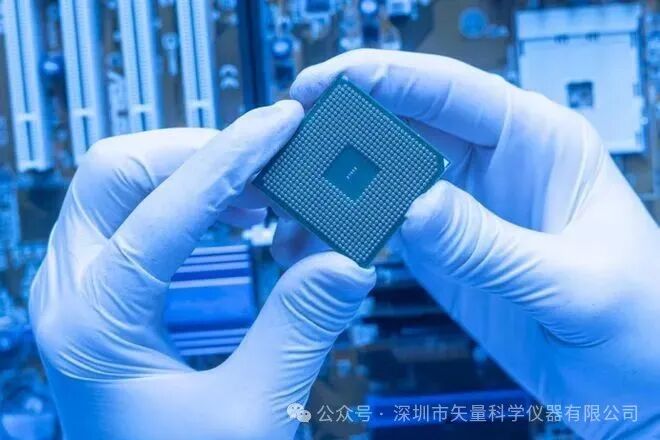
Tape-out is by no means an overnight success! From submitting the final design files to receiving testable sample chips, it usually takes 3 to 6 months. The specific cycle depends on:
-
The complexity of the chip design
-
The advancement of the selected process technology
-
The foundry’s current capacity load
This process includes hundreds of precise steps such as wafer preparation, photolithography, etching, ion implantation, thermal treatment, thin film deposition, chemical mechanical polishing, testing, and packaging, all interlinked and time-consuming.
04
The economic logic behind tape-out: Risks and Returns
The enormous cost of tape-out essentially shifts most of the fixed costs (especially the masks) required for chip mass production onto the small batch samples during the validation phase. This is a high-risk “gamble”:
-
Success: Means that the design has passed validation, allowing for confident mass production, with the high initial tape-out costs being diluted in mass production.
-
Failure: If the chip’s functionality, performance, or yield does not meet standards, it means that the huge investment (mask costs, foundry fees, months of time) goes down the drain, which can be a devastating blow to the design company (especially startups).
Conclusion

Tape-out is a thrilling leap from the “blueprint” to “reality” for chips. It is not only a test of technology but also a competition of financial strength. The high costs mainly stem from the exorbitant masks (especially for advanced processes), the complex wafer manufacturing processes, expensive equipment depreciation, and the disadvantages of small batch production. The long cycles and huge risks of failure further highlight the importance of early verification and simulation work in chip design. Understanding tape-out is essential to truly grasp the difficulties of chip manufacturing and the high costs of chip R&D.

About Us
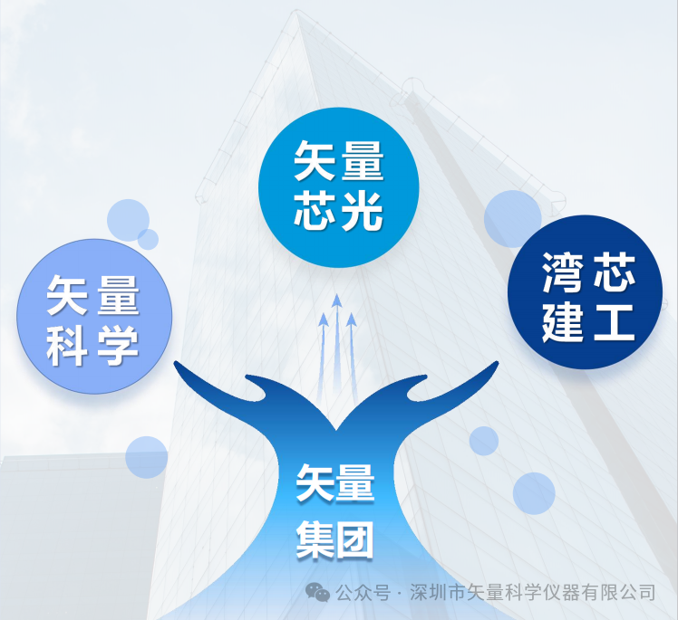
“Vector Chiplight” is a subsidiary of “Vector Group” focused on semiconductor technology, becoming a trusted “semiconductor technology partner” for clients with its superb technology.
-
Providing “turnkey” services from R&D, tape-out to testing for startups, accelerating product realization;
-
Offering customized R&D support for frontier technology explorers, jointly exploring new fields;
-
Providing specialized technical supplements for mature manufacturers.
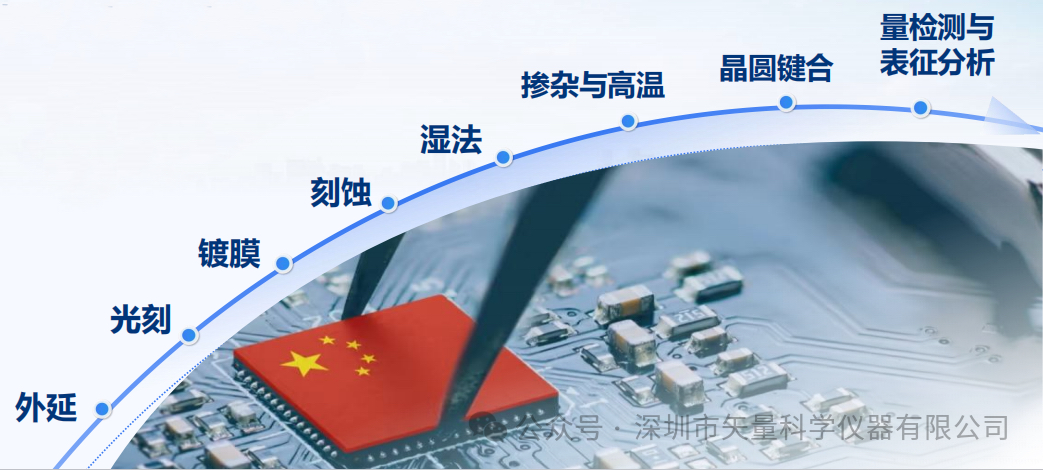
“Vector Chiplight” has the capability of device reverse engineering, simulation, layout design, process development to mass production collaboration; it possesses full-process capabilities from material epitaxy to device preparation, supporting the R&D and pilot production of GaN RF/power/MICRO LED devices and MEMS chips.
<img src=”https://mmbiz.qpic.cn/mmbiz_png/4UnjJ025onCsF6mugKed4OD2pkaItHIAsVcNRpAlibRjy0Dyia1GcTzDp4GZYsmrxk8fxBic5b3mREPibgr4VNQnbQ/640?wx_fmt=png&randomid=rlcq1qmd&watermark=1″