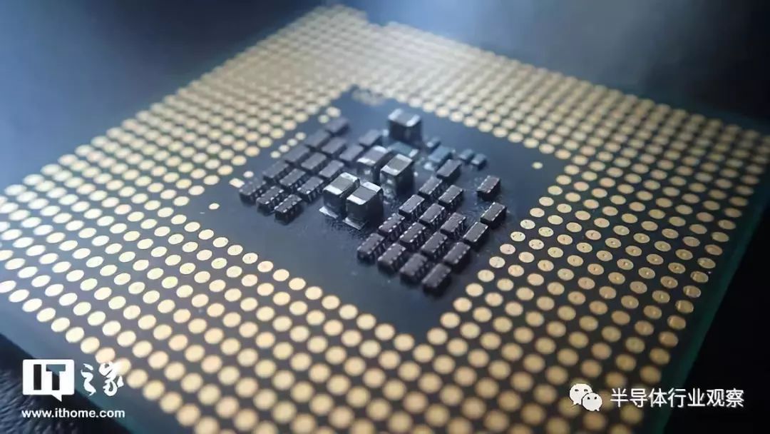
Source: Semiconductor Industry Alliance
Currently, there are two types of civilizations in the world: one is the carbon-based civilization formed by human society, and the other is the silicon-based civilization composed of various chips—because almost all chips are made from single crystal silicon, the total number of chip systems far exceeds the number of humans by dozens or even hundreds of times. Within the chip family, there are various types of chips, ranging from the tons of logic gates built from vacuum tubes to today’s super data centers. The development of electronic technology has gone through generations, and today, various chips are flourishing, with chip manufacturers competing fiercely.
However, among so many chips, there are those specifically for computation, those for control, and those for storage… When classified by the scale of integrated circuits, there are ultra-large scale, large scale, and the older medium and small scale. Specifically, there are CPUs, SoCs, DSPs… With so many chips, distinguishing them clearly takes some effort. This article will guide you to understand some basic integrated circuit chips used for data processing.
Among these chips specifically used for data processing, the most commonly used is the microprocessor system composed of microprocessors, ranging from a small microcontroller to the strongest processor in the world with dozens of cores in a data center, all developed from simple microprocessor systems. Microprocessors are the most widely used chips. Understanding microprocessors and microprocessor systems is very helpful for understanding various chips and control systems that follow.
Microprocessor System
The microprocessor system encompasses various types of computers, microcontrollers/microcontroller units. The total number of microprocessor systems in the world far exceeds the total number of humans. Its basic working principle is to control the behavior of the system using programs.
The basic operational process of a microprocessor system involves the Central Processing Unit (CPU) continuously fetching instructions from memory and executing them, achieving comprehensive management of the system.
1. CPU Structure and Function
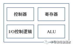
▲Figure: CPU Structure
1) Controller: Completes instruction reading, storing, decoding, and execution.
2) Registers: Temporarily store addresses and data generated during addressing and computation.
3) I/O Control Logic: Responsible for the logic related to input/output operations in the CPU.
4) Arithmetic & Logic Unit (ALU): The core of the processor, responsible for performing arithmetic, logical, and shift operations, used for numerical calculations and generating memory access addresses.
CPU Functions:
1) Exchange information with memory.
2) Exchange information with I/O devices.
3) Receive and output necessary signals for the normal operation of the system, such as reset signals, power supply, input clock pulses, etc.
2. Structure of Microprocessor Systems
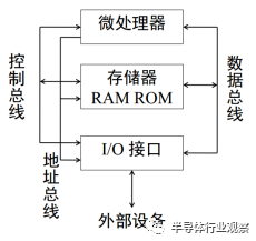
▲Figure: Structure of Microprocessor Systems
1) The external characteristic of the CPU is a limited number of input/output pins.
2) Data Bus: Used for transferring data between the CPU and memory or I/O interfaces, allowing bidirectional communication; the number of data bus lines determines the maximum number of bits that can be exchanged between the CPU and memory or I/O devices at once, which is a criterion for the bit width of the microprocessor. For example, the Intel 386DX and ARM Cortex-M3 are 32-bit microprocessors; processors using Intel’s IA-64 architecture and PowerPC 970 are 64-bit processors; similarly, there are older 8-bit and 16-bit processors.
3) Address Bus: The CPU outputs address codes through the address bus to select a specific memory unit or register that serves as an I/O port, allowing unidirectional communication; the number of address bus lines determines the number of address bits, thus determining the size of the memory space. For example, if the address bus width (number of lines) is 8, it can address 2^8 = 256 memory units. If each memory unit has a word length of 8 bits, the maximum memory space that can be connected to the system is 256kB.
4) Control Bus: Used to transmit control information sent from the CPU or status information from peripherals to the CPU, allowing bidirectional communication;
The programming language of microprocessor systems: A programming language is used to define computer programs and send instructions to the processor through code. Programming languages allow developers to accurately provide the data used by the computer and precisely control the actions to be taken in different situations. The earliest programming languages emerged after the invention of computers, initially used to control Jacquard looms and automatic pianos. Thousands of different programming languages have been invented in the computer field, and new programming languages continue to emerge each year. Many programming languages require instructions to specify the computing program, while some belong to declarative programming, specifying the desired results without stating how to compute.
Machine Language: Each statement in machine language is an instruction that the processor can execute directly, represented in binary sequences of 0s and 1s, corresponding to high and low levels of digital circuits. The machine code of different processors varies, and the specific functions completed will also differ. A program written with the machine instructions of one computer cannot be executed on another computer.
Example: (For illustration only, does not represent real hardware machine code)
Instruction Machine Code:
0000’0000 STORE
0000’0001 LOAD
Address Machine Code:
0000’0000 Register R0
0000’0001 Register R1
Advantages: Functions correspond directly with code, allowing the CPU to execute directly, resulting in the highest efficiency.
Disadvantages: Only binary sequences of 0s and 1s, tedious and difficult to identify.
Assembly Language: Uses concise letters and symbols to replace a specific machine language instruction—binary sequences of 0s and 1s: mnemonic (Memoni) replaces the opcode, and address symbols (Symbol) or labels (Label) replace address codes. Assembly language corresponds directly with machine language, so it is also highly dependent on computer hardware.
Example: Addition Operation (semicolon indicates comments)
MOV R1,? R3;
Assign the value of register R3 to R1
LDR R2, [R4]
; Assign the value of the memory space corresponding to the address represented by register R4 to R2
ADCS R0, R1, R2
; Add registers R1 and R2 with the previous carry value and store it in register R0
Advantages: Assembly statements correspond directly with machine language; mnemonics and labels are often related to actual meanings, making them more intuitive and easier to understand, with execution efficiency similar.
Disadvantages: Different processors have different instruction sets, leading to poor portability; even simple data processing (such as addition, simple sorting, etc.) requires a large amount of code, making the workload for solving practical problems exaggerated and costly.
High-Level Language: Uses expressions close to mathematical or human language to describe programs.
Characteristics: Compared to machine language and assembly language designed for machine development, high-level languages have higher readability and significantly reduced code volume; high-level languages generally avoid direct hardware manipulation, making them safer. Some high-level languages can use assembly language interfaces to control hardware; high-level languages have many mature, easy-to-use, and portable data structures and algorithms, greatly simplifying the development process, saving development costs, and making maintenance easier. They develop rapidly, have complete communities, and allow for easy assistance in solving various problems encountered. Many high-level languages, each with unique characteristics for solving different field problems and well-developed, are available for developers to choose from, such as: Basic, which is suitable for beginners to understand programming concepts; C/C++, which is highly efficient and close to hardware control, suitable for system, hardware driver programming, and embedded development; Java, which is excellent for cross-platform and portability; C#.NET, which can quickly develop projects with Visual Studio; Python, increasingly favored for data analysis and artificial intelligence; Q# developed by Microsoft for future quantum computing; and others. Languages like MATLAB, HTML, and JavaScript, used in various fields, can also be referred to as high-level languages.
Example: Addition Operation
int a = 1, b = 2, c;
c = a + b;
Advantages: Independent of hardware, good portability; suitable languages can be selected for different occasions, leading to high development efficiency.
Disadvantages: Does not directly use hardware, requiring compilation-linking execution or interpretation, not utilizing specific hardware characteristics, resulting in lower efficiency compared to machine language and assembly language; inherent characteristics prevent high-level languages from completely replacing machine language and assembly language in low-level design.
It can be seen that the core component of the microprocessor system is the CPU. The essence of using the microprocessor system to control external devices is to use software programming methods to control external devices. Since the CPU is already a complete, encapsulated component, system designers can only control external devices by writing software, which is then translated into machine-understandable code through compilers or interpreters. The CPU does not have dedicated hardware circuits to fully control the operation of external devices. This implementation method is software-based and is a general implementation, where control signals are transformed from software to hardware through several conversions. However, sometimes, engineering and design fields often require high-speed, high-performance chips to achieve control and computation, which necessitates more powerful CPUs or parallel collaboration of multiple CPUs, increasing costs. At this point, it may be worth considering designing dedicated hardware to meet work requirements.
3. Application-Specific Integrated Circuits (ASIC)
Application-Specific Integrated Circuits (ASIC) are integrated circuits designed for specific purposes. They are designed and manufactured according to specific user requirements and the needs of specific electronic systems. ASICs are characterized by being tailored to specific user needs and have advantages over general-purpose integrated circuits, such as smaller size, lower power consumption, increased reliability, improved performance, enhanced confidentiality, and reduced costs during mass production.
ASICs are divided into full-custom and semi-custom. Full-custom design requires designers to complete all circuit designs, including all processes of chip design, which requires a lot of manpower and resources, offering good flexibility but low development efficiency. If the design is ideal, full-custom ASIC chips can operate faster than semi-custom ones. Semi-custom ASICs use standard cell libraries, allowing designers to select SSI (Small Scale Integration, such as gate circuits), MSI (Medium Scale Integration, such as adders, comparators, etc.), data paths (such as ALUs, memory, buses, etc.), and even system-level modules (such as multipliers, microcontrollers, etc.) and IP cores, which are already laid out and designed for reliability, making it easier for designers to complete system designs.
Today, ASIC design increasingly uses programmable logic devices, with lower development thresholds and difficulties, simplified processes, and reduced costs, leading to richer and more diversified business opportunities. Currently, ASICs have entered high-tech fields such as deep learning, artificial intelligence, and 5G mobile communication technology, and with the promotion of the two major programmable logic device giants, Xilinx and Altera, it is foreseeable that the future of ASIC design will be dominated by programmable logic devices, especially Field Programmable Gate Arrays (FPGAs).
4. Programmable Logic Devices (PLD)
Programmable Logic Devices (PLD) are a type of general-purpose integrated circuit, a subset of ASICs, where logical functions can be determined by programming the device by the user. Generally, PLDs have high integration levels, sufficient to meet the design needs of general digital systems. Designers can program a digital system to be “integrated” onto a single PLD without needing to ask chip manufacturers to design and produce ASICs since the unit cost of designing and manufacturing ASICs is high if the chip demand is low.
PLDs differ from general digital chips in that the digital circuits inside PLDs can be planned after leaving the factory and can even be changed indefinitely, while general digital chips have their internal circuits determined before leaving the factory and cannot be changed afterward. The recent Intel chip vulnerability incident that gained significant attention is due to the inability to change the internal circuits of the CPU, necessitating the design of new CPU chips to resolve the issue or sacrificing some performance to compensate with software fixes.
5. Development History of Programmable Logic Devices
The earliest Programmable Logic Device (PLD) was the Programmable Read-Only Memory (PROM) made in 1970, which consisted of fixed AND arrays and programmable OR arrays. PROM uses fuse technology, can only be written once, and cannot be erased or rewritten. With technological advancements, ultraviolet erasable PROMs (UVEPROM) and electrically erasable PROMs (EEPROM) subsequently emerged. Due to their low cost, slow speed, and ease of programming, they are suitable for storing functions and data tables.
Programmable Logic Arrays (PLA) appeared in the mid-1970s, consisting of programmable AND arrays and programmable OR arrays, but due to the high cost of devices, complex programming, and low resource utilization, they did not see widespread application.
Programmable Array Logic (PAL) was first introduced by MMI in the United States in 1977. It uses fuse programming and consists of programmable AND arrays and fixed OR arrays, manufactured using bipolar technology, allowing for high operating speeds. Due to its flexible design and variety of output structures, it became the first widely used programmable logic device.
Generic Array Logic (GAL) was first invented by Lattice in 1985, featuring electrically erasable, reprogrammable, and configurable encrypted bits. GAL is fully compatible with PAL in practical applications, thus almost completely replacing PAL and can replace most standard SSI and MSI integrated chips, leading to widespread use.
Electrically Erasable Programmable Logic Devices (EPLD) were introduced by Altera in the mid-1980s, based on UVEPROM and CMOS technology, later evolving into PLDs made using EECMOS processes. The basic logic unit of EPLD is the macro unit, which consists of programmable AND arrays, programmable registers, and programmable I/O units. In a sense, EPLD is an enhanced version of GAL, significantly increasing the number of output macro units, providing a larger AND array, greatly improving integration density, and having fixed internal wiring and small delays, which is beneficial for high-frequency operation, but with weaker internal interconnection capabilities.
Complex Programmable Logic Devices (CPLD) were introduced in the early 1990s after Lattice proposed online programmable technology (SP) in the late 1980s. CPLD includes at least three structures: programmable logic macro units, programmable I/O units, and programmable internal wiring, developed on the basis of EPLD, manufactured using EECMOS processes, with significant improvements in logic macro units and I/O units compared to EPLD.
Field Programmable Gate Arrays (FPGA) were first launched by Xilinx in 1985, a new type of high-density PLD made using CMOS-SRAM technology. The structure of FPGA differs from gate array PLDs; it consists of many independent programmable logic modules (CLBs), which can be flexibly interconnected. The functionality of CLBs is strong, capable of implementing logic functions and can also be configured into more complex forms like RAM. Configuration data is stored in SRAM within the chip, allowing designers to modify the logic functions of the device on-site, hence the term “field-programmable.” After FPGA appeared, it was widely welcomed by electronic design engineers and developed rapidly.
Both FPGA and CPLD feature flexible architecture, high integration, and wide applicability. These devices combine the advantages of simple PLDs and general gate arrays, capable of implementing large-scale circuits, with flexible programming. Compared to ASICs, they offer shorter design development cycles, lower design and manufacturing costs, advanced development tools, no need for testing of standard products, and stable quality. Users can repeatedly program, erase, and use, or achieve different functions with different software without changing the peripheral circuits, and can perform real-time online verification.
CPLD is a more complex logic element than PLD. It is a digital integrated circuit that users can construct logic functions according to their needs. Compared to FPGA, CPLD provides relatively fewer logic resources, but the classic CPLD architecture offers excellent combinational logic implementation capabilities and predictable on-chip signal delays, making it ideal for critical control applications.
FPGA is a product developed further from PAL, GAL, EPLD, and other programmable devices. It emerged as a semi-custom circuit in the ASIC field, providing rich programmable logic resources, easy-to-use storage, computational function modules, and good performance, overcoming the shortcomings of custom circuits while addressing the limitations of original programmable devices with limited gate counts.
FPGA and CPLD each have their own characteristics due to structural differences. FPGA has a higher proportion and number of internal flip-flops, giving it an advantage in sequential logic design, while CPLD, with abundant OR gate resources and non-volatile program retention, is suitable for simple circuits focused on combinational logic. Overall, due to the rich resources and powerful functions of FPGA, it stands out in product development applications. Currently, newly launched programmable logic device chips are primarily FPGA-based, and with advancements in semiconductor technology, their power consumption is decreasing, and integration levels are increasing.
In microprocessor systems, software designers use programming languages to control the normal operation of the entire system, while in the field of programmable devices, the objects of operation are no longer groups of data types but hardware devices, such as memories, counters, and even lower-level components like flip-flops and logic gates. Some may even require precise control at the level of integrated transistor switches. Moreover, many devices no longer operate sequentially in a blocking manner but work in parallel, making classic program flow control ideas unsuitable in the field of programmable devices. Designers need to use a language capable of constructing hardware circuits, namely Hardware Description Language (HDL).
6. Hardware Description Language
Hardware Description Language (HDL) is a language that describes logic circuits and systems using formal methods. With this language, the design of logical circuit systems can be described layer by layer (from abstract to concrete) to express the designer’s ideas, using a series of hierarchical modules to represent extremely complex logical systems. Then, using Electronic Design Automation (EDA) tools, simulation verification is performed layer by layer, and the necessary modules to be converted into actual circuits are combined and transformed into gate-level circuit netlists by automatic synthesis tools. Next, using ASIC or FPGA automatic layout and routing tools, the netlists are converted into the specific circuit routing structures to be implemented. According to statistics, currently, over 90% of ASICs and PLDs in Silicon Valley, USA, are designed using hardware description languages.
The development of hardware description languages has a history of over 30 years, successfully applied in all design stages: modeling, simulation, verification, and synthesis. By the 1980s, hundreds of hardware description languages had emerged, greatly promoting and advancing design automation. However, these languages generally target specific design fields and levels, and the multitude of languages can confuse users. Therefore, a universally accepted standard hardware description language that is multi-domain and multi-level is needed. In the late 1980s to the 1990s, VHDL and Verilog HDL languages adapted to these requirements and became standards set by the Institute of Electrical and Electronics Engineers (IEEE).
Now, with the emergence of ultra-large-scale FPGAs and SoC core FPGA chips, the coordination of hardware and software design and system design is becoming increasingly important. Traditional hardware design is increasingly inclined to combine with system design and software design. Hardware description languages have rapidly evolved to adapt to new situations, leading to the emergence of many new hardware description languages, such as System Verilog, SystemC, Cynlib C++, etc.; on the other hand, PLD design tools have increasingly added support for traditional high-level design languages (like C/C++) in addition to hardware description language design inputs.
Currently, hardware description languages are flourishing, including VHDL, Verilog HDL, Superlog, SystemC, System Verilog, Cynlib C++, C Level, etc. Overall, VHDL and Verilog HDL are still the most widely used in PLD development fields. As the scale of logical system development continues to grow, system-level hardware description languages like SystemC and System Verilog are also seeing increasing applications.
VHDL
As early as 1980, due to the U.S. military industry’s need for a method to describe electronic systems, the U.S. Department of Defense began developing VHDL. In 1987, IEEE established VHDL as a standard. The reference manual was the IEEE VHDL Language Reference Manual Draft 1076/B, approved in 1987, known as IEEE 1076-1987. However, initially, VHDL was merely a standard for system specification, not specifically for design. The second version was developed in 1993, known as VHDL-93, which added some new commands and attributes.
Although there is a saying that “VHDL is a $400 million mistake,” VHDL was indeed the only hardware description language standardized before 1995, which is an undeniable fact and advantage; however, its use is relatively cumbersome, and its synthesis libraries have not yet been standardized, lacking the ability to describe transistor-level simulation designs. Currently, for very large system-level logic circuit designs, VHDL is more suitable.
In essence, the underlying VHDL design environment is supported by device libraries described in Verilog HDL, making interoperability between them crucial. Currently, two international organizations, OVI (Open Verilog International) and VI, are planning this work, preparing to establish a dedicated working group to coordinate the interoperability of VHDL and Verilog HDL languages. OVI also supports direct expression from VHDL to Verilog without translation.
Verilog HDL
Verilog HDL was first created in 1983 by Phil Moorby of GDA (Gateway Design AUTOMATION) company. Phil Moorby later became the main designer of Verilog-XL and the first partner of Cadence company. Between 1984 and 1985, Phil Moorby designed the first simulator called Verilog-XL; in 1986, he made another significant contribution to the development of Verilog HDL by proposing the XL algorithm for fast gate-level simulation.
With the success of the Verilog-XL algorithm, Verilog HDL language rapidly developed. In 1989, Cadence acquired GDA, and Verilog HDL became Cadence’s proprietary property. In 1990, Cadence decided to make Verilog HDL public and established the OVI organization to promote the development of Verilog HDL language. Based on the advantages of Verilog HDL, IEEE established the IEEE standard for Verilog HDL in 1995, namely Verilog HDL 1364-1995; in 2001, the Verilog HDL 1364-2001 standard was released, which included the Verilog HDL – A standard, giving Verilog HDL the ability to describe analog design.
SystemC
With the rapid development of semiconductor technology, SoC has become the direction of integrated circuit design today. The processors in smartphones and tablets are essentially SoCs, as they integrate CPUs, Graphics Processing Units (GPUs), Digital Signal Processors (DSPs), Baseband processors, etc. In various designs of system chips (like system definition, hardware/software partitioning, design implementation, etc.), the integrated circuit design community has been considering how to meet the design requirements of SoC, continuously searching for a system-level design language that can simultaneously achieve a high level of software and hardware description.
SystemC was developed in this context, collaboratively developed by Synopsys and Coware to respond to the current demand for system-level design languages. On September 27, 1999, over 40 world-renowned EDA companies, IP companies, semiconductor companies, and embedded software companies announced the establishment of the “Open SystemC Alliance.” The well-known company Cadence also joined the SystemC Alliance in 2001. Since the establishment of the alliance in 1999, SystemC has been updated from version 0.9 to 1.0, 1.1, and finally to the latest version 2.0 in October 2001.
7. Common Data Processing Chips
Having sorted out the concepts and principles of two major categories (microprocessors and ASICs) of chips, let’s now understand some common chips.
MCU
The most common microprocessor system in daily life is the microcomputer around us, which is personal computers (PCs), including desktops, laptops, or the new stars of the PC world—various cool 2-in-1 devices. These seemingly complex electronic systems evolved from the simplest microprocessor systems. However, daily life does not require so many computers. For example, to create an electric rice cooker that can automatically control heating and insulation, its CPU performance may only require a fraction of what a computer needs, and it does not need complex input/output devices. In design, unnecessary parts can be largely discarded, and the CPU, clock generator, Random Access Memory (RAM), Read-Only Memory (ROM), and necessary external devices can be integrated into a small chip, referred to as a microcontroller or microcontroller unit (MCU). Currently, MCUs are the most widely used electronic control chips, and their control programs can be downloaded to ROM using special burning tools to perform system functions. These ROMs can be PROM, UVEPROM, EEPROM, etc. If the MCU does not integrate ROM, it can also connect to external ROM. According to system architecture, microprocessor systems can be divided into Von Neumann architecture (also known as Princeton architecture) and Harvard architecture, differing in how programs and data are stored. Similarly, MCU chips can also be divided into these two structures, flexibly meeting needs.
MPU
The Microprocessor Unit (MPU) integrates many CPUs to process data in parallel. In simple terms, MCUs integrate RAM, ROM, and other devices; MPUs do not integrate these devices and are highly integrated general structures of central processing unit matrices, which can also be considered as MCUs without integrated peripherals.
PLD (CPLD/FPGA)
Since the widely used PLDs are CPLD and FPGA, these two types of chips will be introduced as examples. As previously mentioned, the internal structure of CPLD/FPGA is completely different from that of CPUs; the internal circuits can be modified multiple times, and different combinational logic circuits and sequential logic structures can be formed according to user programming. They are “universal” chips. CPLD/FPGA may look like a CPU; however, using CPLD/FPGA for control is a pure hardware implementation, essentially no different from a digital logic circuit built with thousands of basic logic gates. Therefore, it is possible to directly use HDL programming in CPLD/FPGA to build a “CPU” (sometimes with hard cores and soft cores, which will not be elaborated on due to space constraints), and then set up the corresponding I/O and buses, creating a simple microprocessor system. However, this also transforms it into software control, negating the hardware control advantages of PLD. Thus, CPLD/FPGA are often used in conjunction with actual CPUs, where more complex algorithmic circuits are programmed onto CPLD/FPGA, and when the CPU encounters these complex tasks, it hands them over to CPLD/FPGA for processing. Once processing is completed, the results are returned to the CPU, enhancing the overall performance of the control system.
ADC, DAC
Physical quantities in nature can be divided into analog and digital quantities. Analog quantities have continuous values within a certain range, and their count is infinite; digital quantities have discrete values within a certain range, and their count is limited. Computers can only process discrete digital quantities, so analog signals must be transformed before they can be processed by computers. This transformation, which converts physical quantities in nature into continuously varying currents or voltages (hence the term “analog”), samples under the conditions of the Nyquist Sampling Theory (also known as Shannon Sampling Theory), obtaining time-domain discrete signals, which are then quantized (linear and nonlinear quantization) into digital signals, and finally encoded into binary 0s and 1s for computer processing. This transformation is called Analog-to-Digital Conversion (A/D), and the corresponding circuitry can be integrated into a chip, known as Analog Digital Circuit (ADC). Similarly, there are Digital-to-Analog Conversion (D/A) and Digital Analog Circuit (DAC) chips, which also need to satisfy relevant theorems in mathematics and information theory during D/A conversion.
DSP
A Digital Signal Processor (DSP) is a specialized chip used for high-speed processing of digital signals.
The digital signals converted through ADC often involve large data volumes, making direct processing by the CPU inefficient, especially as the CPU has to perform many general computing tasks. Therefore, dedicated circuits are often used for processing digital signals, such as digital filtering, Fast Fourier Transform, time-frequency analysis, and processing of voice and image signals.These computations are often complex, involving numerous additions and multiplications of complex numbers. For example, the calculation of discrete Fourier transform is quite complicated, but using the Fast Fourier Transform algorithm can greatly reduce the computational workload, although the circuitry involved is complex.Integrating circuits capable of performing these complex computations onto a single chip allows for performing a multiply-accumulate operation in one clock cycle, enabling complex computations like base-2 FFT butterfly operations, audio filtering, and image processing. Such chips are called DSPs. DSPs are also a special type of CPU, particularly suitable for signal processing, such as in 3G Node B, where DSPs are extensively used for signal processing. DSPs outperform CPUs in handling streaming media, and nowadays, voice signals on smartphones are processed by DSPs. The concept of DSP is becoming increasingly blurred, as architectures like ARM9 resemble DSPs more than CPUs. Many chips now integrate DSPs, GPUs, baseband processors, etc., with more traditionally discrete chips being integrated together for collaborative work to improve efficiency and reduce energy consumption, which is also a trend for the future.
SoC
With the rapid development of semiconductor technology, mobile internet, and smart terminals, the development of traditional microprocessor systems can no longer keep pace with the times. Modern information technology urgently requires a chip with multiple functions, strong performance, and low power consumption to meet the needs of an increasing number of smart devices. SoC has thus emerged.
SoC stands for System on a Chip, which means integrating an entire information processing system onto a single chip, known as a chip-on-board system or system-level chip. This definition is not entirely clear now, as the components integrated into SoCs vary depending on their intended use. Generally speaking, SoCs are complete systems that possess the full functionality of an entire digital system. They are also a type of ASIC, containing a complete control system along with embedded software.
SoC also represents a technology aimed at achieving system functionality through the collaborative development of various modules’ hardware and software, ultimately integrating the results into a single chip. Due to their rich functionality and the requirement for impressive performance, SoCs have become the most feature-rich hardware, integrating CPUs, GPUs, RAM, ADC/DAC, modems, high-speed DSPs, and various other chips. Some SoCs must also integrate power management modules and control modules for various external devices, fully considering the distribution and utilization of various buses… Nowadays, SoCs in smartphones integrate the aforementioned components along with baseband processors and many related communication modules.
Compared to traditional microprocessor systems, the circuitry of SoCs is more complex, naturally raising the requirements for design and manufacturing processes, and significantly increasing dependence on collaborative hardware/software development. To date, only top companies in the semiconductor industry possess the capability to design and manufacture SoCs independently. Currently, in the field of performance- and power-sensitive terminal chips, SoCs dominate, with powerful, always-on SoCs serving us in the smartphones we use daily. Even traditional software giants like Microsoft have launched Windows operating systems based on Qualcomm’s Snapdragon 835 platform. Moreover, the applications of SoCs are expanding into broader fields, with increasing applications in industries such as drone technology, autonomous driving, and deep learning. Achieving a complete electronic system with a single chip is the future development direction of the semiconductor and IC industries.

Official Account ID: imecas_wx