Scientific discoveries often begin with unexpected small events, and the discovery of OLED is no exception. One night in 1979, Dr. Qinyun Deng, a Chinese scientist working at Kodak, suddenly remembered he had left something in the laboratory while on his way home. When he returned to the lab, he found an organic battery used for experiments glowing in the dark! This unexpected surprise marked the beginning of OLED’s birth, and Dr. Deng was henceforth known as the “Father of OLED”.

In 1990, researchers at the University of Cambridge, including Burroughes and Friend, discovered that the conductive polymer material PPV exhibited excellent electroluminescent properties. They successfully developed a method to apply polymer materials to OLEDs using a coating process, creating polymer OLED devices, also known as Polymer LEDs or PLEDs. Due to the thermal stability, flexibility, and mechanical processing capabilities of polymer materials being superior to those of small organic molecules, and the simpler manufacturing process of the devices, polymers are gradually becoming a new research hotspot in the field of organic EL.
In 1992, Heeger and others first invented flexible displays made from plastic substrates, showcasing the most captivating aspect of organic electroluminescent displays to the world.
In 2007, Sony’s first OLED TV, the XEL-1, was officially launched on December 1. Many retailers were busy promoting OLED sales, but due to a monthly production of only 2,000 units and about 700 dealers across Japan, the actual sales exceeded expectations, leading to severe shortages at the time.
By 2012, Samsung had already invested in one 4.5-generation line, three 5.5-generation lines, and one 7.5-generation AMOLED production line.
At the 2012 CES, both Samsung and LG launched 55-inch OLED TVs.
In 2013, LG added an 8.5-generation WRGB OLED TV panel production line.
On August 6, 2010, Skyworth and South China University of Technology jointly established Guangzhou New Vision Company, focusing on OLED display technology.
Five Major Advantages of OLED Organic Panels
1. Excellent Self-Emission:
1) Infinite Contrast Ratio
OLED produces deeper blacks and brighter whites, with clear and strong three-dimensional contrast, without any halo effect;
Traditional LED-backlit LCD TVs have a contrast ratio of 5000:1. Their blacks appear grayish, with average picture depth, and the images appear washed out and hazy.
2) Ultra-Wide Viewing Angle
OLED has a viewing angle of 160 degrees, allowing for color-accurate images to be viewed from any angle;
In standard brightness half-value angle conditions, LCD panels have a viewing angle of only 100 degrees, with noticeable color distortion after moving more than 50 degrees from the center.
3) Ultra-Fast Response Speed
OLED has a response speed of 0.001ms, presenting clean and sharp images without trailing;
LCD (IPS VA) panels have a response time of 4-5ms, resulting in trailing effects. The reason: Liquid crystal molecules have viscosity and take time to pivot, making improvements difficult. Currently, the most widely used techniques to improve display image application include developing new liquid crystal materials, using overdrive techniques, and employing frame interpolation techniques.
2. Perfect Picture Quality Even on Daily Channels
We have been conducting comparative experience events, comparing the image effects of OLED TVs and LCD TVs when playing daily channel content. The results fully demonstrate the advantages of OLED in contrast, viewing angles, and response speeds, with strong three-dimensional depth, good color saturation, and natural reproduction, making it very suitable for the human eye. This has been certified by Tsinghua University’s Color Research Institute.
3. True Curved Panels
When OLED panels are made into curved shapes, the solid self-emitting materials maintain uniformity, and each pixel can independently control whether to emit light, showing no light leakage when viewed from the front or side, fully reflecting the perfect angle advantage. In contrast, LCD (VA) panels, when made into curves, have internal liquid crystal molecules that change arrangement, leading to noticeable light leakage and poor viewing angles.
4. Truly High-End Brand Design
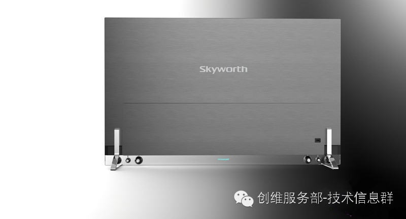
Ultra-thin: The thickness of a 55-inch TV is 4.x mm (LCD TVs reach 10 mm);
Ultra-light: The weight of a 55-inch module is 5.x kg (LCD TVs can weigh 20 kg or more);
5. Eye Health
OLED TVs have the advantage of emitting less blue light compared to LCD TVs, which is more beneficial for vision protection and eye health.
Knowledge Related to OLED Screens
1. Concept of OLED Liquid Crystal Screens;
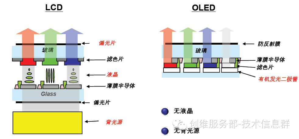
OLED (Organic Light Emitting Display) liquid crystal screen, unlike LCD screens, does not require a backlight. This screen uses a very thin coating of organic materials and a glass substrate. When current passes through, these organic materials emit light.
According to driving methods, OLED products mainly include Passive Matrix OLED and Active Matrix OLED.
A: Active Matrix OLED (AMOLED) has a complete cathode layer, organic molecular layer, and anode layer, with the anode layer covered by a thin-film transistor array, forming a matrix. The TFT array itself is a circuit that determines which pixels emit light, thus defining the image composition;
B: Passive Matrix OLED (PMOLED) consists of cathode strips, organic layers, and anode strips. The anode and cathode strips are perpendicular to each other. The intersection points of the cathode and anode form pixels, which are the emitting parts. The external circuit applies current to the selected cathode and anode strips, determining which pixels emit light and which do not.
Currently, OLED products mainly use active matrices.
2. Principle of OLED Emission: OLED Screens (Compared to LCD)
OLED is a self-emitting product that does not require a backlight or liquid crystal like LCD.
2. Principle of OLED Emission:
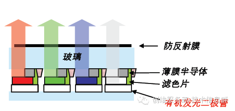
Display Principle: Based on the data of digital images, thin-film semiconductors control the electrodes of each pixel on the panel, exciting the organic light-emitting diode materials in each pixel to emit light. Each pixel emits light according to the data of the digital image, forming recognizable image signals for the human eye.
Material Composition:
The main materials composing an OLED module include: glass (substrate), backplane, and rare metals (panel circuitry TFT, light-emitting diodes).
OLED Light Control
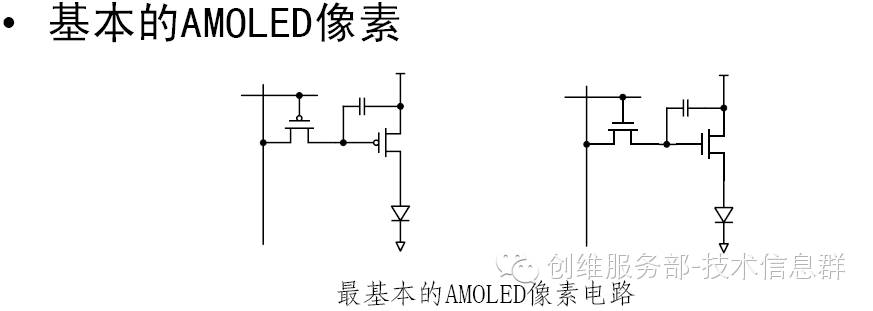
The TFT transistor acts like a controlled switch. In the diagram, Tsw serves as the switch, with the source S of Tdr connected to the power supply VDD. A capacitor Cst is applied between the source S and gate G, keeping Tdr in a controlled ON state. When the gate of Tsw is activated by the scanning signal Gn, the source drive signal DATA is applied through Tsw to the gate of Tdr, charging Cst and converting it into the drain current of Tdr to control the driving of OLED pixels. For the entire display, Gn controls the switching of Tsw to select the required rows, while the source DATA drive circuit provides grayscale control signals.
3. Recovery Mechanism of OLED Screens:
Due to the drift characteristics of the TFT, long-term operation can lead to noticeable drift in the TFT device, resulting in color distortion in the display.Currently, LG’s screens have predetermined voltages for the gray level current I required by each pixel. If there is drift, the voltage required to achieve current I will differ. If the voltage for current I is set at V2, the voltage required for drift to A would need to be V1. If V2 is still applied, the current will exceed the actual required value.
According to the principle of the TFT, using different polarities of gate bias can monotonically increase or decrease the threshold voltage drift. Therefore, to recover the TFT, the gate voltage of the driving transistor Tsw cannot always maintain one polarity (positive bias stress). A single polarity of gate voltage leads to the generation of states in the TFT in one direction, causing the threshold voltage drift to change in a single direction. Therefore, during recovery, it is necessary to provide each pixel with a signal with the opposite polarity to the normal working data, within certain voltage limits, and the magnitude of the value is related to the drift degree of each TFT.
Scan to Get More Content