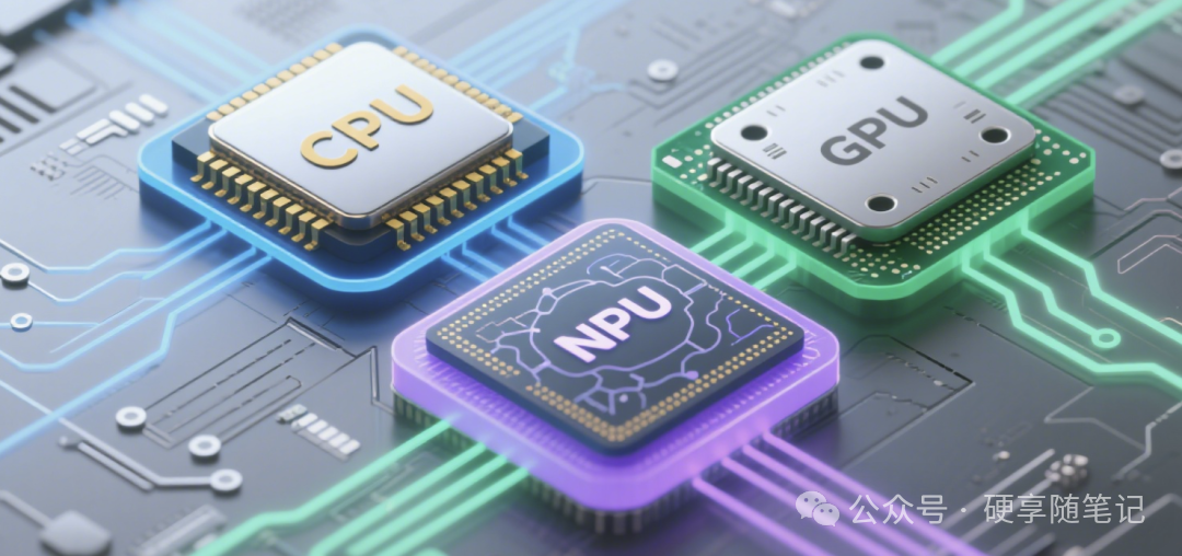
 Figure 1Let’s start by explaining these three terms: CPU, NPU, and GPU;CPU: Central Processing Unit (CPU) is thecore of thecomputer systemforcomputationand control, serving as the finalexecution unitforinformation processingand program execution.NPU: Neural Processing Unit (NPU) is an embedded intelligent computing chip specifically designed for digital multimedia processing.GPU: Graphics Processing Unit (GPU), also known as a display core, display chip, or video processor, is a co-processor used for processing images and graphics calculations, widely used in personal computers, workstations, and some mobile devices (such as smartphones and tablets).
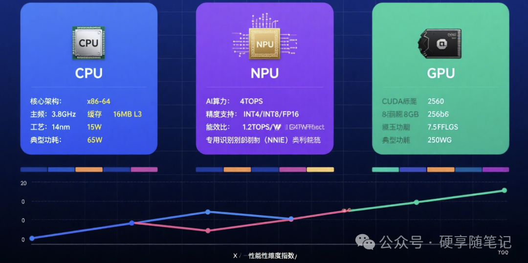 Figure 2The differences among the three are clear in their definitions: the CPU handles “computational tasks”, the GPU handles “display tasks”, and the NPU handles “neural tasks”. The CPU primarily focuses on simple data processing and program execution; the NPU is mainly for intelligent computing; and the GPU is primarily for image processing. As shown in the table below:
| Dimension | CPU | NPU | GPU |
| Full Name | Central Processing Unit | Neural-network Processing Unit | Graphics Processing Unit |
| Design Goal | General computation, logical control | Specialized acceleration for neural networks | Graphics rendering → General parallel processing |
| Core Count | Few (2–64) butlarge cores | Mostly matrix/vector units | Very many (thousands) small cores |
| Architecture Features | Large cache, complex branch prediction | Storage-computation integration, synaptic weight arrays | SIMD/many ALUs, high parallelism |
| Strengths | Operating systems, databases, serial logic | CNN/Transformer inference, edge AI | Graphics, scientific computing, AI training |
| Power Consumption | Medium | Very low (high energy efficiency) | Higher |
| Representative Products | Intel Core, AMD Ryzen | Huawei Ascend, Apple Neural Engine | NVIDIA RTX, AMD Radeon |
Figure 3Next, let’s look at three other terms:DMIPS (Dhrystone Million Instructions executed Per Second) measures the number of million instructions executed per second, indicating the processing capability of the system within one second.TOPS (Tera Operations Per Second) represents that 1 TOPS means the processor can perform one trillion (10^12) operations per second.TFLOPS (teraFLOPS) equals one trillion (10^12) floating-point operations per second. FLOPS (Floating-point operations per second) indicates the number of floating-point operations per second.
| Metric | Unit | Measured Content | Typical Scenario |
| DMIPS | 10⁶ integer instructions / second | General integer performance of CPU | MCU, mobile SoC, embedded control |
| TOPS | 10¹² arbitrary operations / second (mostly multiply-accumulate) | Integer/fixed-point computing power (INT8/INT4, etc.) | NPU/AI accelerator inference, autonomous driving chips |
| TFLOPS | 10¹² floating-point operations / second | Floating-point computing power (FP16/FP32/FP64) | GPU scientific computing, AI training, graphics rendering |
Figure 4How are DMIPS, TOPS, and TFLOPS calculated?DMIPS Calculation (Measured Value)
- Compile the Dhrystone source code (C language) to run on the target CPU.
- DMIPS = Dhrystones per Second ÷ 1757
This means DMIPS is either tested in practice or tested by manufacturers; for example, the Snapdragon 8 Gen 1 has a CPU performance of approximately 560 K DMIPS as provided by the manufacturer.TOPS Calculation (Theoretical Value)TOPS = Clock Frequency × Multiply-Accumulate Unit Count × Operations per Unit per Cycle ÷ 10¹²Where
- Clock frequency is in GHz (1 GHz = 10⁹ Hz);
- Multiply-accumulate operations (MAU, MAC) are the physical units within the chip that can perform parallel multiply-accumulate operations for neural network acceleration, including many operations (such as convolution, dot product, matrix operations, digital filter operations, and even polynomial evaluations);
- Operations per unit per cycle is commonly 2 (one multiplication + one addition);
- Finally, divide by 10¹² to convert the result to “trillions per second”.
TFLOPS Calculation (Theoretical Value)TFLOPS = Core Count × Clock Frequency (GHz) × Floating-point Operations per Cycle ÷ 1000
- Core Count;
- Clock Frequency;
- FP32 Operations per Cycle: 2 (one FMA = multiply + add)
For example, to calculate the FP32 TFLOPS of the NVIDIA RTX 5090, the formula is: CUDA core count × Boost clock frequency × 2 (FMA operation),which equals 21760 × 2.407 GHz × 2 = 104.752 TFLOPS.Additionally, the Tensor Core of the RTX 5090 has a computational capability of:
- FP4 dense computation: 680 (Tensor cores) × 2.407 GHz × 512 × 2 ≈ 1,676 TOPS;
- FP4 sparse computation: 680 × 2.407 GHz × 1024 × 2 ≈ 3,352.084 TOPS (close to the 3,352 AI TOPS published on the official website).
In summary, the FP32 computing capability of the RTX 5090 is 104.752 TOPS, and its Tensor Core’s FP4 sparse computing capability is approximately 3352.084 TOPS; Figure 5Why do many chips now frequently mention TOPS?This is the reason: because NPUs primarily handle AI acceleration inference and autonomous driving tasks, in the current environment of large models, everyone is very concerned about this parameter, which also represents a kind of technical capability.Does a high TOPS necessarily mean strong performance?As mentioned earlier, there is a difference between “transmission rate” and “transmission data”; the same applies here. For example, TOPS represents the processing capability of the chip, and the TOPS computing power we commonly refer to is calculated based on INT8. Let’s assume everyone calculates this data in this way. This is just a theoretical value; in practice, many factors affect it, such as the bandwidth of the DDR used, throughput, and the frequency used in the circuitry. Therefore, we rarely see actual TOPS performance being showcased. Simply put, the chip’s capability also requires hardware and software collaboration to achieve maximum performance.Note: There is a difference between theoretical and actual values; actual values are affected by memory bandwidth, power walls (influenced by power and temperature, leading to forced frequency reduction and core shutdown), and utilization rates. Measured values typically only reach peak values of 30–70%; just like the smartphones and computers we use, we can clearly feel that when the temperature reaches a certain level, they become sluggish. I have encountered CPUs that have frequency reduction or core shutdown operations; we call this method Thermal Management. This is also something that many “storytellers” mention when presenting data, but there will be a small note below stating “XXX data is measured by XX laboratory, actual usage may vary slightly, all based on XX data.”
Disclaimer:
This account maintains neutrality regarding all statements and views in original and reprinted articles, and the articles are provided solely for readers’ learning and communication. The copyright of the articles, images, etc., belongs to the original authors. If there is any infringement, please contact for deletion. WeChat ID: Hard Sharing NotesWelcome to share and progress together—— The End ——