Source | EETOP
Author | William G. Wong
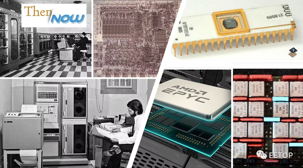
The UNIVAC I, 70 years ago, was actually the second commercial computer; it had a liquid mercury delay line memory that could store 1,000 words of 12 alphanumeric characters. It operated at low megahertz speeds and could read 7,200 decimal digits per second. The concept of a computer small enough to fit in your palm that could communicate wirelessly with the rest of the world seems like something from science fiction, like ray guns and flying cars. The development of these other projects has not progressed as quickly as processor technology, but we have them all now.
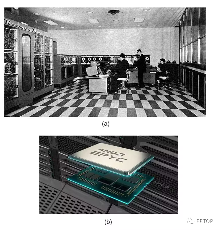
Comparison of the UNIVAC series from 70 years ago with AMD processors
AMD processors are based on 5-nanometer transistor technology that operates at gigahertz (GHz) speeds. In contrast to early mainframes that required kilowatts of power and forced air or even water cooling, their power consumption is about a few hundred watts. UNIVAC used 125 kW and weighed 13 tons. Multi-chip servers typically have thousands of gigabytes to tens of thousands of gigabytes of external storage, not to mention on-chip registers and multi-level cache systems.
The processors and computer architectures of the time were just beginning to develop. The UNIVAC 1103A was the first computer with interrupt capabilities. Input was typically through punch cards, paper tape, or magnetic tape, while output usually included a roll of 132-column paper (14 inches wide, 10 characters/inch, plus margins). Flashing status lights were not LEDs, and rows of toggle switches were standard.
Mainframe
Mainframes were typically installed in special rooms, and raised flooring for wiring and cooling became the norm for decades. The famous International Business Machines (IBM) System/360 (S/360) began in 1964 (see Figure 2). The S/360 replaced five other IBM computer series.
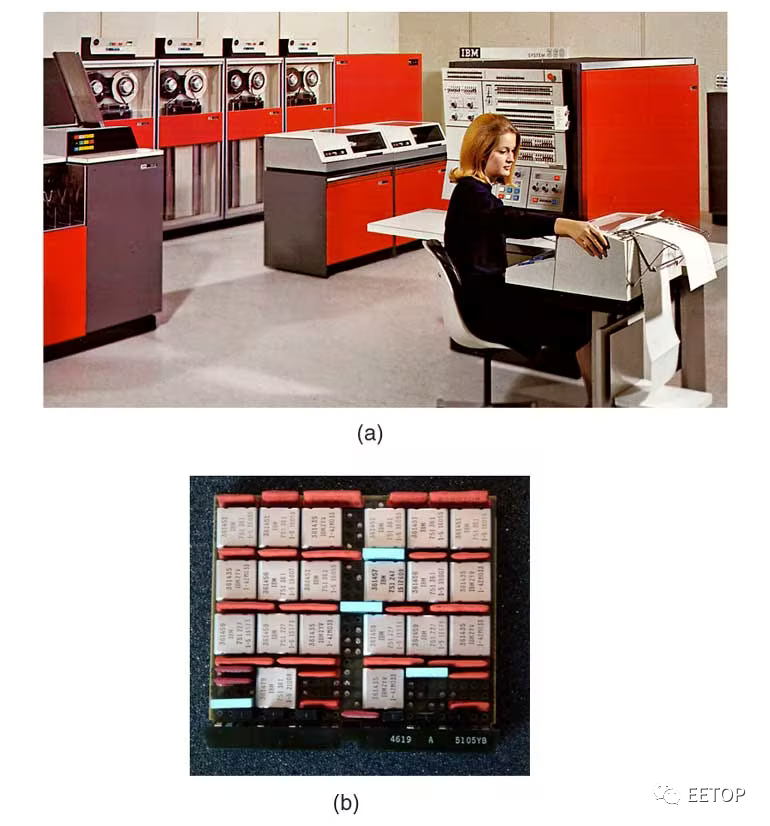
IBM System/360 (a) revolutionized mainframes. (b) Shows the chips of the 360
The S/360 introduced IBM’s Solid Logic Technology (SLT). This packaging technology combined custom hybrid circuits, including discrete, flip-chip mounting, glass-encapsulated transistors and diodes, and silk-screened resistors on ceramic substrates. The basic architecture started with 16 32-bit registers, 8-bit bytes, and 24-bit addressing. The EBCDIC character set was the preferred encoding, now ASCII has become the recognized standard. Nine-track magnetic tape was ubiquitous, and eventually the IBM 3340 “Winchester” disk drive joined the mix.
“BUNCH” (Burroughs, UNIVAC, NCR, Control Data, and Honeywell) plus IBM, along with programming languages like FORTRAN and COBOL, joined assembly language to make processor programming easier.
Operating systems were typically written in assembly language, but the Burroughs B5000 mainframe was programmed in Algol. The Burroughs ESPOL (Executive System Problem Oriented Language) algorithm variant provided system access and was used to write the Master Control Program (MCP). These mainframes had no assembly language. The C programming language did not become popular until much later. The term MCP was later used as the name of the antagonist in the “Tron” movie series.
I want to mention the B5500 because it was one of the first mainframes I used. It had a descriptor and stack-oriented architecture implemented in hardware (see Figure 3). It also used tag words to distinguish between data and code. The B6500 moved to an 8-bit variable-length instruction set.
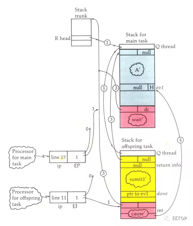
Burroughs mainframes implemented descriptor and stack-oriented architecture in hardware.
Multiprocessor systems are common, but each processor is usually a box or board. While mainframes still exist, they have migrated to the latest multicore chip technology.
Minicomputer
The desire to shrink computers and make them more accessible turned mainframes into minicomputers, which could come from mainframe companies as well as DEC, Data General, HP, Prime Computers, and Wang.
A typical minicomputer is 16 bits and weighs about 50 pounds; it does not require a custom room, though air conditioning helps. You could purchase one for just $10,000. They were made using off-the-shelf LSI technology. The 7400 series transistor-transistor logic (TTL) logic chips were a popular implementation device. These chips are still available, but are no longer used to implement processors.
I used a dual-processor version of the HP 2000 minicomputer (see Figure 4) in high school. It was a time-sharing system that could accommodate dozens of teletypes with optional punch tape units and eventually CRT monitors. Long-distance connections provided by 300 and 1200 baud modems were the norm.
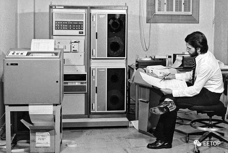
The 16-bit HP 2100 minicomputer had 16 kB of magnetic core memory and used tape for removable storage.
The 12-bit DEC PDP-8 was a popular platform, and the 16-bit PDP-11 eventually became the LSI-11 chip set.
Microprocessor
Microprocessors compatible with minicomputers could be used. The 8-bit microprocessor that ultimately drove the personal computer (PC) revolution can be traced back to the Intel 8008, which was succeeded by the Intel 8080, using a 40-pin dual in-line package (DIP) (see Figure 5). The initial clock frequency was 2 MHz, and instructions required at least four cycles to complete. There was no cache, pipelining, or multithreading at the time.
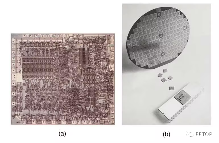
The 8-bit Intel 8080 sparked the PC revolution. Shown are the 8080 (a) and the 8080 on wafer, as a chip and in its package (b).
The 8080 implemented using N-channel metal-oxide-semiconductor logic (NMOS) and non-saturating enhancement-mode transistors as loads. It was compatible with 5V TTL. The MPU had 8-bit registers that could be combined into 16-bit registers. A 16-bit stack pointer provided a recursive environment.
The Intel 8080 was the core of the IMSAI 8080 microcomputer (as shown below), which appeared in the movie “WarGames” and was mentioned in “Ready Player One.” The Intel 8085 was a single-voltage, 5V part that was succeeded by the Zilog Z80. The Z80 was widely used and adopted by many products.
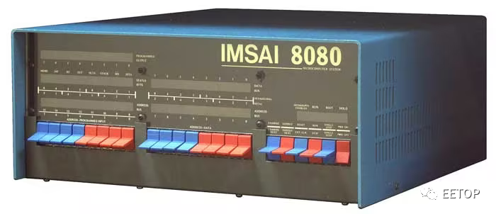
The IMSAI 8080 was built around the 8080 processor
Intel was not the only company with microprocessors. A host of other 8-bit and 16-bit microprocessors, such as the Motorola 6800 and MOS Technology 6502, found applications in everything from the Atari 2600 to the Apple II.
However, it was the 16-bit Intel 8088 and 8086 that pioneered the personal computer era with IBM.
The 8088/86 architecture was designed to facilitate the transition from the 8080, but their instruction sets and source code were not compatible. This is in stark contrast to the x86 compatibility we know today.
Current Architecture
The performance of processors has increased significantly, and their sizes have decreased. 8-bit, 16-bit, and even 32-bit microcontrollers in BGA packages are now common, with sides only a few millimeters. They typically feature on-chip clocks, flash memory, serial and parallel interfaces, as well as analog-to-digital and digital-to-analog converters. Some even have on-chip sensors for testing temperatures and more.
This is a far cry from the first single-chip microcontroller I used, the Intel 8748, which was an 8-bit processor with UV EPROM (see Figure 7). The current NXPKinetis KL03 uses a 2-mm 2-chip-level package (CSP). The 32-bit Cortex-M0+ runs at 48 MHz and has 32-kB flash memory, while the Intel 8748 had an 11-MHz clock that provided 0.73 MIPS through a 2-kB UV EPROM.
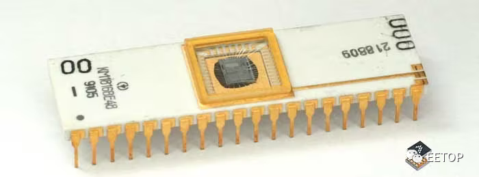
The 8-bit, 0.7-MHz 8748 microcontroller in a 40-pin package is large.
Packaging is also changing the way processors are combined. 2.5D and 3D stacking have been widely used for memory and high-end processors. There are also wafer-based solutions, such as those from Cerebras Systems, which can use trillions of transistors focused on machine learning algorithms.
The choices available to developers today are vastly different from just a few years ago. From small microcontrollers to chips designed for cloud-based servers, multicore processor chips are readily available. Processor architectures include x86, Arm, MIPS, RISC-V, SPARC, and POWER. Among these, x86 and Arm currently dominate with the rise of RISC-V.
The use of a large number of transistors has made it possible to create system-on-chip (SoC) solutions with many different processors—an incredible variety. Similarly, features using dedicated processors for everything from security to network management are now common.
The rise of the Internet of Things (IoT) and IoT devices has driven the demand for secure processors and on-chip secure storage. Sometimes a dedicated communication processor is added to the mix, and low-power processors are used to enhance higher-performance processors while reducing computational demands. Low-power options have led to always-on operations, so there is really no off button these days.
While I focused on the basic central processing unit (CPU) architecture, we should not overlook the vast number of new architectures, such as graphics processing units (GPUs), FPGAs, and programmable accelerators for tasks like machine learning. General-purpose GPUs (GPGPUs) share multi-chip communication links with CPUs. GPU programming elevates single instruction, multiple data (SIMD) and vector computing to another level, with software developers now mixing target platforms for optimal performance.
Original Article
https://www.electronicdesign.com/altembedded/article/21213779/electronic-design-processors-have-come-a-long-way
Editor: Lu Dingci