 👆If you would like to meet regularly, feel free to star 🌟 and bookmark it~
In the rapidly growing artificial intelligence market over the past few years, besides NVIDIA, another chip winner has emerged: SK Hynix. According to financial data, SK Hynix achieved revenue of $16.23 billion in the second quarter of 2025, with profits reaching $5.1 billion, a year-on-year increase of 69.8%. This has allowed them to surpass Samsung, which has held the top position for decades, becoming the world’s leading DRAM supplier.
Among them, HBM, which accounts for 77% of revenue, is the most important asset that has enabled SK Hynix to reach its current position.
As a special type of DRAM, HBM utilizes vertical stacking and connects to the processor through fine lines called TSV (Through-Silicon Vias) within the silicon chip. Since TSV allows for direct connections between multiple HBM DRAM chips, it can significantly increase overall memory bandwidth. This advantage has made HBM play a crucial role in the era of large model training. However, the accompanying cost pressures are also evident.
Thus, in the inference era, GDDR has found its opportunity.
Artificial Intelligence Has Changed
In fact, before the emergence of large models, artificial intelligence had already undergone a long evolution and exhibited different characteristics. For example, traditional AI primarily focused on data analysis and prediction based on input models, limited to a finite set of input/output modalities (e.g., text to web results).
According to Nidish Kamath, Director of Semiconductor IP Product Management at Rambus, this stage of artificial intelligence can be referred to as the AI 1.0 era. Typical AI applications during this phase include voice assistants, recommendation engines, and search platforms, which excel at handling relatively simple tasks (such as voice-to-voice, text-to-text, and voice-to-text) but struggle with complex and diverse content creation, such as music across multiple models.
Subsequently, with the arrival of large models, artificial intelligence officially entered the AI 2.0 era.
Because LLMs can understand complex inputs (including text, images, or speech) and generate outputs ranging from traditional text responses to more advanced forms (such as code, images, videos, or even 3D models). These features have opened up infinite creative and innovative possibilities across multiple modalities in the AI 2.0 era. These characteristics are reflected in LLMs such as GPT-4, PaLM2, ERNIE 4.0, Inflection-2, Gemini 1.5, and Olympus, and are expanding into more edge and endpoint application scenarios.
Nidish Kamath points out that the rapid development of AI 2.0 applications places enormous demands on memory bandwidth and capacity for AI training and inference workflows. For example, in AI training, the corresponding scale of AI models is rapidly expanding: the 175 billion parameters of Chat GPT-3 pale in comparison to the 1.76 trillion parameters of Chat GPT-4, highlighting the continuous growth in demand for memory bandwidth and capacity.
At the same time, many AI applications are migrating from data centers to edge and endpoint devices, which raises higher requirements for existing memory systems. As a result, GPUs using GDDR memory have become the preferred choice for inference engines.
This has also allowed GDDR to find opportunities in more AI inference chips.
GDDR, Seizing the Opportunity
As the name suggests, GDDR (Graphics Double Data Rate) was originally designed as a memory specifically for GPUs, necessary for high-speed data transfer required for rendering graphics. In practical applications, GDDR can operate on both the rising and falling edges of the clock cycle, effectively doubling the data transfer rate. Thus, each GPU has dedicated GDDR memory, managed by a memory controller to optimize data flow and reduce latency. Over time, new versions have improved bandwidth and efficiency, enhancing overall graphics performance.
“Compared to HBM, its cost-performance characteristics make it suitable for large-scale deployment in edge networks and IoT endpoint devices,” says Nidish Kamath. He further points out that HBM employs 2.5D/3D architecture, providing higher total throughput and better per-watt bandwidth efficiency for AI/ML and HPC applications with wider interfaces and lower clock frequencies (compared to GDDR7). However, its implementation costs are higher and more complex, which may not be necessary for less intensive tasks. Additionally, AI inference applications typically use optimized model parameters with lower precision than during training. This means that their requirements for memory and total bandwidth are lower compared to training infrastructure.
At this point, GDDR7 perfectly meets these requirements. According to the standard announced by JEDEC last March, GDDR7 single-chip data rates can reach up to 192GB/s, with chip densities of up to 32Gb and the latest data integrity features. This high data rate is achieved by using PAM3 (Pulse Amplitude Modulation) with three levels (+1, 0, -1) to transmit 3 bits over 2 cycles, while the current GDDR6 generation uses NRZ (Non-Return-to-Zero) to transmit 2 bits over 2 cycles.
“On one hand, it can provide high bandwidth at lower memory capacity points; on the other hand, its simpler packaging compared to HBM also reduces the overall memory cost of GDDR7 systems—an important factor for deploying inference systems that may be larger in scale than AI training,” Nidish Kamath tells Semiconductor Industry Observer.
Nidish Kamath also acknowledges that designers have multiple memory options for AI inference applications. Given the long history of successful applications of DDR4 memory in laptops and desktop systems, initial systems adopted this well-tested technology. Today, DDR5 memory has also become an option. Another choice is LPDDR, which has been deployed in billions of mobile phones, with its latest generation being LPDDR5X.
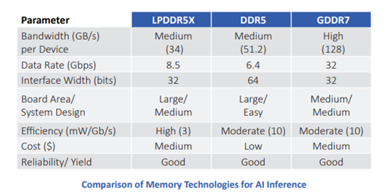
“In terms of this critical parameter of bandwidth, GDDR7 memory performs exceptionally well. A GDDR7 device configured with a data rate of 32 Gbps and a 32-bit wide interface can provide 128 GB/s of memory bandwidth, more than double that of any alternative. GDDR7 memory offers the best combination of speed, bandwidth, and latency performance for AI inference applications,” emphasizes Nidish Kamath.
In response to this new trend, Rambus is fully committed.
Rambus’s IP Empowerment
As a leading Silicon IP and chip provider in the industry, with 35 years of technological leadership, Rambus has built three major semiconductor solutions based on innovation, including foundational technologies, semiconductor IP, and chips. In terms of foundational technologies, Rambus has developed approximately 2,800 patents over 35 years; in semiconductor IP, Rambus offers two categories of leading products, including interface IP and security IP; in chip products, Rambus provides all the chipsets required for DDR4 and DDR5 memory modules, except for DRAM chips.
It is also on this accumulated foundation that Rambus has introduced the GDDR7 controller.
According to Nidish Kamath, to enhance memory bandwidth, GDDR7 uses PAM3 signaling to replace NRZ (PAM2) signaling. This new scheme allows memory to transmit “3 bits of information” over two cycles, increasing the data transfer volume by 50% compared to GDDR6 at the same clock frequency, thus raising the actual rate limit to 40 Gbps. To ensure reliable data transmission at such high speeds, GDDR7 integrates advanced FEC (Forward Error Correction) mechanisms. This helps mitigate the signal integrity challenges inherent in high-frequency operations and PAM3 signaling.
“Through PAM3 signaling, a fully functional, bandwidth-saving memory implementation solution is provided, elevating GDDR7 memory’s data rate to 40 Gbps and throughput to 160 GB/s, driving the use of advanced GDDR memory in cutting-edge AI accelerators, graphics processing, and high-performance computing applications,” Nidish Kamath points out. “As a recognized leader in signal integrity (SI) and power integrity (PI), Rambus has over 30 years of experience dedicated to enabling the highest performance systems in the market. With the expertise and assistance of companies like Rambus, designers can better address the signal integrity challenges posed by increased data transmission rates,” Nidish Kamath emphasizes.
Based on this, Rambus has launched the industry’s first GDDR7 memory controller IP with significant advantages, as detailed below:
1. Rambus GDDR7 memory controller IP offers industry-leading GDDR7 performance, with pin rates of up to 40 Gbps, providing 160 GB/s of usable bandwidth per GDDR7 memory device.
2. Rambus’s GDDR7 controller core is designed for applications requiring high memory throughput, high clock frequency, and full programmability.
3. The controller core accepts commands via AXI interface or simple local interface and converts them into the command sequences required by GDDR7 SGRAM devices. It also supports all low-power modes.
4. The core uses advanced scheduling algorithms to reorder user requests in the queue to maximize bus efficiency and minimize memory bus idle time caused by DRAM access rules. The core selects the next best request to process in the queue while maintaining access restrictions and consistency rules, achieving high efficiency and minimizing the latency of all requests. The core uses memory bank management techniques to monitor the status of each GDDR7 SGRAM. It only opens or closes memory banks when necessary, thereby minimizing access latency.
5. This core supports all GDDR7 link features, including PAM3, NRZ signaling, CRC with read/write retries, data scrambling, data poisoning, clamshell mode, and DQ logic remapping.
In summary, the features of the GDDR7 memory controller IP include:
1. Support for operation at rates of up to 40 Gb/s per pin
2. Support for all GDDR7 link features, including PAM3 and NRZ signaling
3. Support for various GDDR7 device sizes and rates
4. Optimized for various traffic scenarios to achieve high efficiency and low latency
5. Flexible AXI interface support
6. Optimized for various traffic scenarios to achieve high efficiency and low latency
7. Reliability, availability, and serviceability (RAS) features, such as end-to-end data path parity, storage register parity protection, etc.
8. Comprehensive memory testing support
9. Support for a collection of customer and third-party physical layers
In addition to the GDDR7 controller IP, Rambus also offers a series of products such as HBM controller IP. With these leading IPs, Rambus has become an indispensable player in the AI chip market.
Click here👆 to follow for more original content
*Disclaimer: The content of this article represents the author’s personal views. Semiconductor Industry Observer reprints it solely to convey a different perspective and does not imply endorsement or support of this viewpoint. If there are any objections, please feel free to contact us.

Recommended Reading
100 trillion, invested in semiconductors
Chip giants, market value plummets
Jensen Huang: HBM is a technological miracle
Jim Keller: RISC-V will definitely win
The 10 highest-valued chip companies globally


If you like our content, please click“View” and share it with your friends~