In the field of power electronics, Gallium Nitride (GaN) power semiconductors are undoubtedly a hot topic today. With their outstanding performance, they are rapidly replacing traditional silicon-based devices. However, in the face of two mainstream GaN transistor variants—cascode D mode GaN and E mode GaN, the cascode D mode mentioned in this article specifically refers to devices that utilize a cascode structure, which is clarified for consistency with the original text.
This white paper published by Renesas Electronics reveals a groundbreaking conclusion through in-depth analysis and detailed data: the cascode D mode GaN is fundamentally the superior platform, demonstrating overwhelming advantages in performance, reliability, versatility, manufacturability, and practical applications. Its secret to success lies in its ability to fully leverage the inherent advantages of GaN materials.
The Natural Gift of GaN: 2DEG
The success of GaN transistors is largely attributed to a key natural phenomenon: *two-dimensional electron gas (2DEG) channels. 2DEG is a high-speed channel that spontaneously forms at the interface between GaN and a thin AlGaN layer. Its electron density is one of the highest naturally occurring densities in semiconductors, and it also possesses an extremely high mobility of up to 2000 cm²/V·s, which is twice that of the most advanced silicon (Si) and silicon carbide (SiC) devices. Therefore, 2DEG brings about an extremely low figure of merit (FOM) for the product of resistance and capacitance, achieving record-high efficiency.
All GaN Power Semiconductors Start with D Mode
Essentially, every GaN power semiconductor starts with D mode. A typical lateral GaN power transistor structure shows that the AlGaN/GaN layers are deposited on a silicon substrate and separated by an engineered buffer layer to achieve high-quality material and high breakdown voltage. Thanks to the properties of the material itself, the 2DEG channel spontaneously forms at the AlGaN/GaN interface without the need for external gate bias. This means that the device is naturally normally-on and requires a negative gate bias to deplete the channel and turn it off. It is, in essence, a depletion-mode (D mode) device.
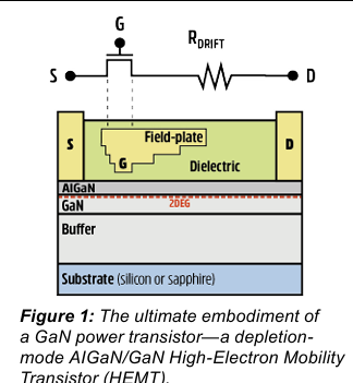
However, power electronic systems require normally-off devices to achieve fail-safe operation. So, how can a lateral GaN HEMT be converted into a normally-off device? This question has led the cascode D mode and E mode (p-GaN gate) technologies down different paths.
In the cascode D mode technology, the GaN HEMT retains its original state to preserve its highest performance and reliability. The 2DEG channel in this natural state can fully utilize its unparalleled combination of high mobility and high charge density. Renesas’ cascode D mode approach pairs the GaN HEMT with a low-voltage, normally-off silicon MOSFET to achieve normally-off operation. This solution provides a forward threshold voltage of 2.5 V to 4.0 V, depending on power level, topology, and system architecture.
In contrast, the E mode method chooses to directly control the 2DEG channel within the GaN HEMT, fundamentally compromising the advantages of 2DEG.
E Mode GaN: Stifling the Natural Advantages of 2DEG
When power engineers modify lateral GaN HEMTs to achieve normally-off behavior, critical compromises are inevitable.
First, the charge density of 2DEG must be reduced, resulting in higher specific area resistance, leading to a lower figure of merit than in its natural state.
Second, a layer of p-type doped GaN must be added beneath the gate metal. This p-GaN layer acts as a built-in negative battery (approximately -3.2 V) to turn off the 2DEG channel, resulting in a weak positive threshold voltage of only 1.6 V.
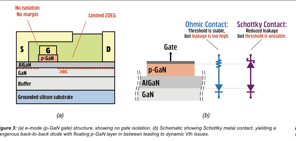
In noisy environments or at high power levels, a threshold voltage of 1.6 V may be completely insufficient. At this point, a negative gate drive of about -3 V may be required, which increases circuit complexity and introduces additional dead time losses. More importantly, the negative drive has a detrimental effect on the device’s dynamic or switching resistance (a critical resistance in applications), which is often not mentioned in the data sheets of E mode devices, raising significant concerns in the industry.
The Domino Effect: Isolation Loss, Dynamic Threshold Issues, and Low Performance in E Mode
The aforementioned modifications in E mode come at a significant cost: the loss of gate isolation. Replacing the gate dielectric with p-type GaN results in the gate no longer being isolated, which can cause significant gate current under positive bias, severely limiting the maximum gate voltage rating. To reduce this significant gate current, another modification is made: changing the gate contact from ohmic metal to Schottky barrier
However, the Schottky barrier introduces another challenge, hindering the discharge of gate-drain capacitance during turn-on transients, leading to a harmful phenomenon known as “dynamic threshold”. Dynamic threshold can cause dynamic on-resistance issues. At 480 V, the dynamic on-resistance of E mode devices increased by 27%, while the corresponding devices in the normally-off D mode only increased by 5%, significantly reducing conduction losses.
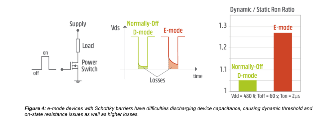
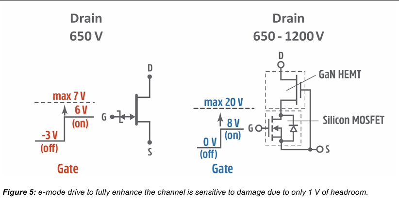
To mitigate this issue, theoretically, the gate can be overdriven to reduce on-resistance, but this faces a very small voltage window, as it must adhere to a very small maximum gate rating (maximum 7 V) to prevent gate damage. In contrast, the normally-off D mode GaN offers a +/-20 V automotive-grade maximum gate rating, providing excellent reliability and high drive margin.
Moreover, as the temperature rises during normal operation, the mobility of 2DEG naturally decreases. This decline also leads to a reduction in the transconductance of the p-GaN gate, resulting in slower transitions and more switching losses. This decline creates a low-efficiency “perfect storm.” To address these issues, the p-GaN gate solution may require larger chip sizes, but this will increase Miller capacitance, reduce overall efficiency, and increase costs.
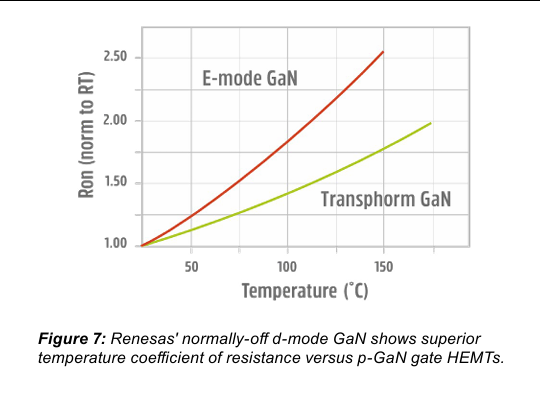
As the data sheets show, E mode devices have a higher temperature coefficient for on-resistance compared to normally-off D mode. Between 25°C and 150°C, the increase can be as much as 2.6 times, leading to a rapid increase in conduction losses.
D Mode: The Right Choice, The Right Approach
The normally-off D mode platform pairs normally-on GaN HEMTs with highly reliable, high-performance normally-off low-voltage silicon MOSFETs to achieve fail-safe operation while retaining the highest performance of GaN and the highest reliability of silicon MOSFET gates. This design philosophy has two important reasons: it works in harmony with the laws of nature and is backward compatible with today’s silicon technology.
Normally-off D mode devices do not face the challenges encountered by E mode devices mentioned above. For example, since it drives a gate-isolated low-voltage silicon MOSFET, it is not affected by dynamic threshold issues. The threshold voltage is set by the silicon MOSFET and is independent of the GaN HEMT. This configuration also brings about a second natural gift of GaN: the SiO2/Si interface. This interface naturally isolates the gate of the device, providing high drive margin and excellent reliability.
Breaking the Myths: Addressing Common Misunderstandings about D Mode GaN
Myth 1: Silicon MOSFETs will increase on-resistance and reverse recovery charge (Qrr).
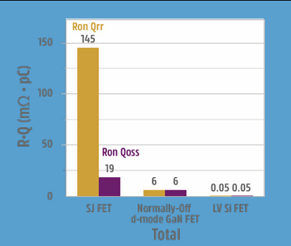
Truth:In the normally-off D mode GaN technology, the GaN chip bears most of the high voltage in the off state (>90%), while the silicon MOSFET only needs to withstand a few tens of volts. Since the specific on-resistance decreases with the square of the rated voltage, the silicon MOSFET achieves extremely low RDS(on), contributing less than 10% of the total on-resistance of the normally-off D mode and having a very small reverse recovery charge (Qrr).
Myth 2: E mode devices have no Qrr.
Truth:When switching from reverse conduction to the off state, the reverse recovery charge includes not only the recombination of minority carriers in bipolar transport but also the formation of the space charge region, which is essentially equivalent to output charge (Qoss). GaN HEMTs do not have reverse conduction bipolar transport, but they still have output capacitance that needs to be charged during reverse recovery. In short, QrrQrr cannot be zero.
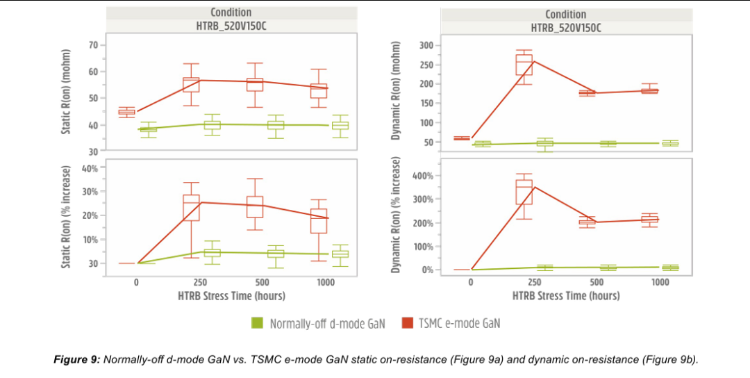
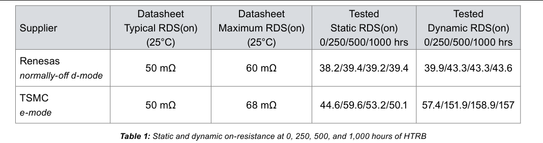
High Voltage Reverse Bias (HTRB) tests further demonstrate the superiority of normally-off D mode. After 1000 hours of HTRB testing at 520 V and 150°C, static and dynamic on-resistance tests were conducted on Renesas’ normally-off D mode devices and TSMC’s E mode devices.
The test results showed that the on-resistance of E mode devices increased by about 30% in static tests, which may be due to charge being trapped in the dielectric layer, requiring a long recovery time to manifest in static tests. More concerning is that in dynamic on-resistance tests, the on-resistance of E mode devices increased by over 300%. This could be due to design, process, or epitaxial issues. In contrast, normally-off D mode GaN devices exhibited excellent stability.
Relying on static on-resistance ratings may not accurately reflect the performance of the device. Dynamic testing is an effective method for measuring charge capture and overall on-resistance stability. The tabulated data clearly indicates that the dynamic on-resistance of E mode devices will not pass AEC-Q101 certification, as its dynamic on-resistance variation exceeds 20%. This could affect its rated current, leading to additional power losses and subsequent reliability issues.
Myth 3: Normally-off D mode GaN will oscillate.
Truth:Normally-off D mode GaN has a high gain, which is an excellent characteristic for achieving fast switching. To prevent oscillation and fully leverage the advantages of any fast-switching semiconductor device, circuit engineers should follow standard design principles, such as minimizing gate and power loop inductance, selecting the correct gate resistance and ferrite beads, and deploying RC snubber circuits when necessary (usually on the DC link). All these design principles are easy to implement and do not degrade the performance of GaN HEMTs; rather, they can enhance it while suppressing oscillation and electromagnetic interference (EMI).
More Advantages: Packaging Versatility and Short-Circuit Tolerance
The normally-off D mode platform can elegantly adapt to various standard packages, such as through-hole, surface mount, and multi-chip modules, further enhancing its performance and reliability. Renesas’ SuperGaN normally-off D mode platform employs chip-on-chip technology and silicon-like wire bonding without adding extra wire bonds or parasitic inductance, allowing for ideal connection schemes. This configuration is also perfectly suited for System-in-Package (SiP), enabling seamless integration of gate drivers and controllers with D mode GaN HEMTs and low-voltage silicon MOSFETs, providing more options for diverse end applications.
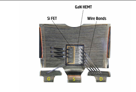
Another key advantage of normally-off D mode GaN HEMTs is that they do not require the source to be connected to the substrate. Floating or insulated substrates enable higher voltage ratings (e.g., up to 1200 V) and bidirectional switching capabilities.
As GaN transistors penetrate the motor drive market, short-circuit capability will become an essential feature. The insulated gate voltage handling capability of D mode allows for very sophisticated design approaches, which have been shown to adjust the short-circuit withstand time (SCWT) of Renesas’ D mode devices to reach 5 microseconds, meeting the requirements of commercially available gate drivers.