01
Overview of SEM IP Functionality
The SEM (Soft Error Mitigation) technology achieves observable soft error simulation through targeted ECC parity bit injection. This mechanism precisely selects parity bits within the Configuration RAM Frame (CRAM Frame) for controllable flipping, ensuring that injected errors are located in the redundant parity area rather than in functional logic bits, thus avoiding interference with the integrity of design functionality. It is primarily applied in demanding scenarios (such as aerospace, industrial control, etc.), where the SEM controller can ensure a higher level of reliability. To determine whether to use SEM IP in the design, one must understand the possibilities and system-level considerations.
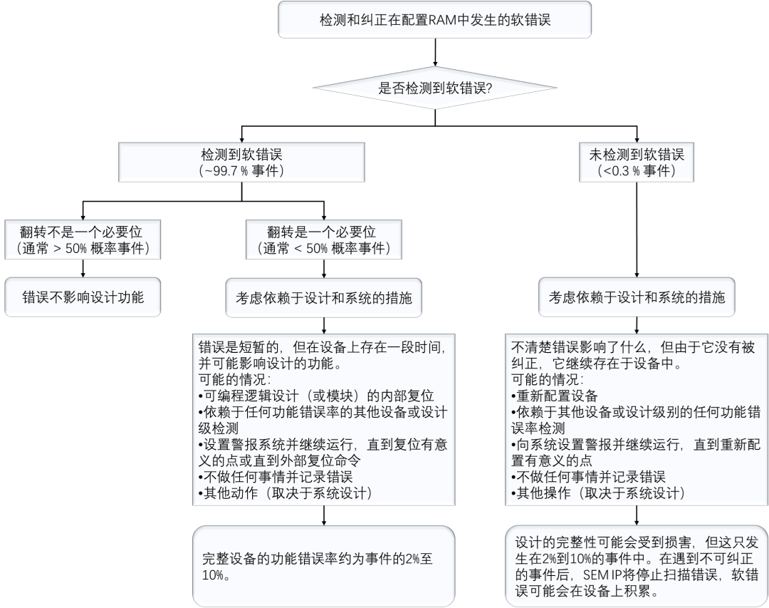
Figure 1. Example of Soft Error Decision Tree
02
SEM IP Interface and Configuration
02.1
Introduction to SEM IP Interface
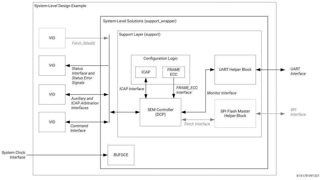
Figure 2. Module Design of SEM Reference Design
The system-level example design encapsulates the SEM controller and channels for interfacing the controller with other devices. Notably, the SEM controller does not have a reset signal. This is because the SEM controller’s task is to monitor and maintain the original configuration state, rather than to restart from some temporary (possibly erroneous) state, hence no reset is set. It automatically initializes itself with internal synchronization reset derived from the global reset signal. The table below provides a detailed description of each interface.
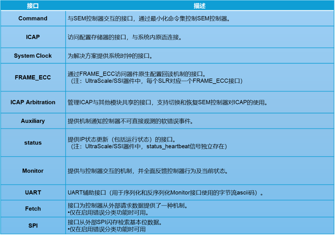
Table 1. Functional Descriptions of Each Interface
02.2
Introduction to SEM IP Configuration
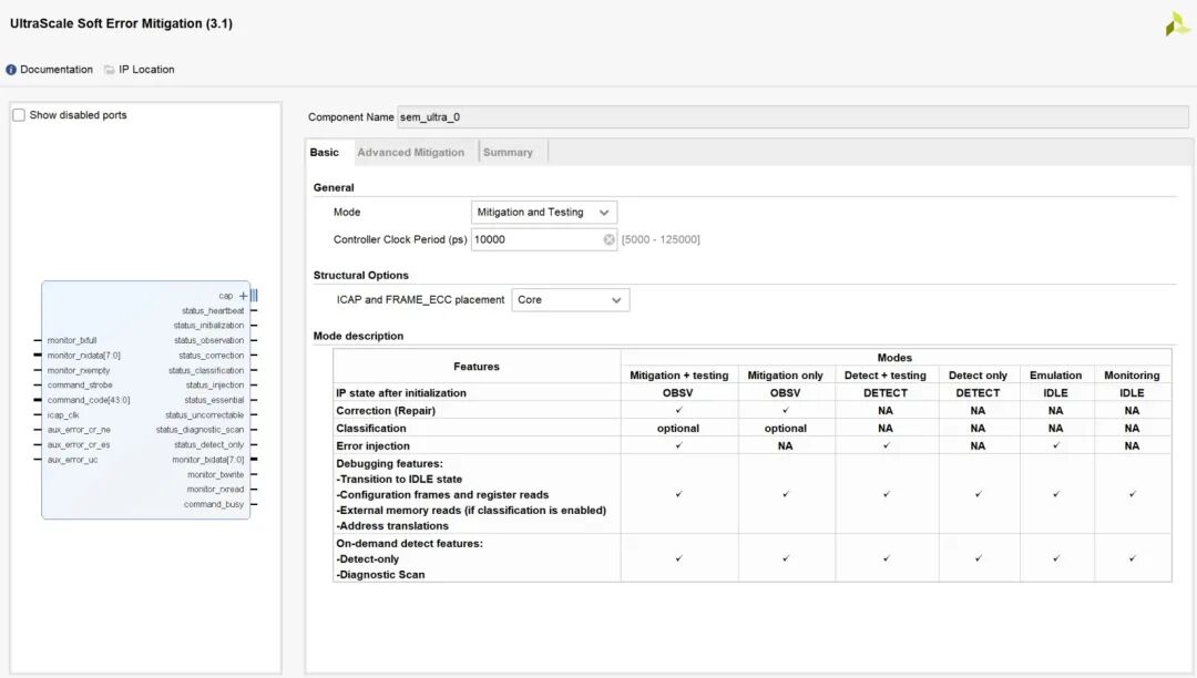
Figure 3. SEM IP Configuration Interface
◾ Controller Modes
Divided by mode:
SEM IP can be divided into six modes:
• Mitigation and Testing
• Mitigation Only
• Detection and Testing
• Detection Only
• Simulation
• Monitoring
According to the characteristics of each mode within the IP, “Mitigation and Testing” is the most suitable mode for testing simulations. The core difference of this mode compared to others is that it supports both error injection and error correction capabilities simultaneously.
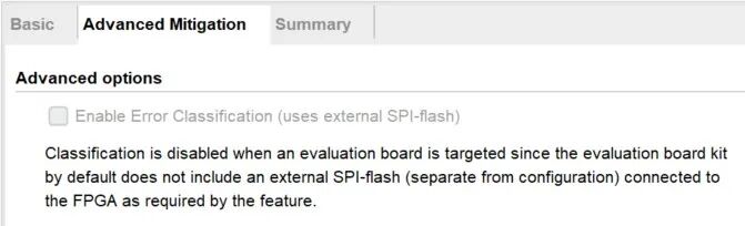
Figure 4. SEM IP Advanced Configuration Interface
The error classification function is only available in error correction modes (Mitigation and Testing/Mitigation Only) to determine whether the corrected soft errors affect design functionality. It is worth mentioning that the IP disables the error classification function by default for development boards because the evaluation board does not include external SPI memory by default.
◾ Controller Clock
The clock cycle of the controller is set through the “Clock period” field; the smaller the value, the higher the frequency, and the shorter the error mitigation time. However, during design, it is necessary to ensure that the target device supports the set period; otherwise, a warning will be triggered. The table below summarizes the ICAP FMax. When the evaluation board is the target, the default controller clock period is automatically selected based on the specific clock frequency provided in the example design’s pins.
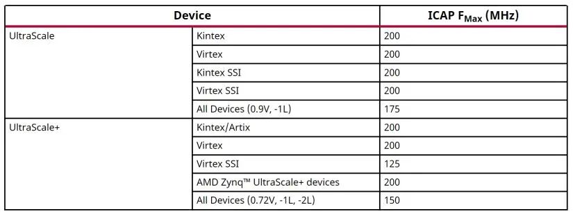
Table 2. Maximum Frequency Supported by ICAP
◾ Controller Structural Options
The inclusion method of primitives (ICAP/FRAME_ECC) in SEM IP configuration is divided into two types, with the core difference being the visibility of the primitives and the control of connections:
1. Included in the Core:
-
Applicable Scenario: When no other logic needs to access ICAP/FRAME_ECC primitives.
-
Features: The primitives are automatically embedded in the core, and the connection is transparent to the user (not exposed as ports).
-
Limitations: Not applicable to UltraScale SSI devices.
2. Included in Example Design:
-
Applicable Scenario: When other logic needs to access ICAP/FRAME_ECC primitives.
-
Features: The primitives are explicitly instantiated at the example design level, requiring the user to manually connect the ports.
03
On-Board Testing
03.1
Test Environment Setup
The project is based on xapp1298
Hardware Platform: MPSoC (ZCU102)
Software Version: Vivado 2019.1, SDK 2019.1
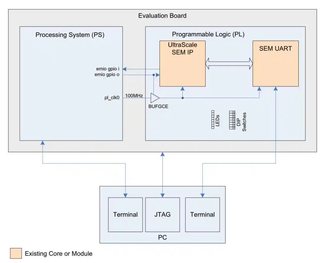
Figure 5. Project Design Schematic Diagram
In this project design, the PS provides the SEM controller with the ICAP clock signal (icap_clk) through a dedicated PL clock interface (pl_clk0), and the ICAP arbitration control and status LED signals are centrally managed through the PS extended EMIO interface.
03.2
SEM IP Debugging
This article is conducted in “Mitigation and Testing” mode, aiming to observe error injection and the IP’s error correction functionality. Key steps involved in the operation of SEM include: transferring PCAP authority to ICAP, clock enabling, ICAP arbitration switching behavior, and debugging methods. The following details these aspects.
◾ Transfer of PCAP Authority to ICAP
Due to the lack of FPGA startup independence, the MPSoC must actively release PCAP authority after PS startup and transfer configuration control to ICAP during debugging. This is because PCAP and ICAP have similar functions, both being PS access configuration control interface, and cannot run simultaneously. Therefore, for MPSoC devices using SEM, it is necessary to modify the register pcap_ctrl (address 0XFFCA3008) bit0 to zero to switch to ICAP control. Otherwise, initialization will fail, causing SEM to be stuck in the “Initialization” state and unable to start error correction functionality.
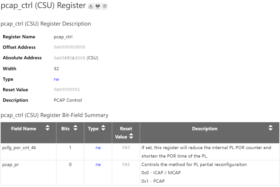
Figure 6. MPSoC pcap_ctrl Register
Two methods can be used to implement register configuration:
1. Add the following code on the PS side

2. Configure the register under XSCT

◾ BUFGCE Enable
Observing Figure 5, it can be seen that the BUFGCE module is integrated into the clock path. The enable port CE of this module is low by default because, under system-level requirements, the clock passed through MMCM/PLL needs to stabilize before being provided to SEM. For example, in some scenarios using MIG, due to the high timing precision required during the BIST phase, using SEM during this phase may probabilistically lead to MIG verification errors, and the enable switch can mitigate this issue.
◾ ICAP Arbitration Switching Behavior
The ICAP arbitration interface implements a mechanism for multiple functions to share ICAP according to the logic in the flowchart below. It is important to note that since the IP does not know whether the configuration memory was manipulated when access to ICAP is stopped, it may lead to reinitialization and reboot upon subsequent access.
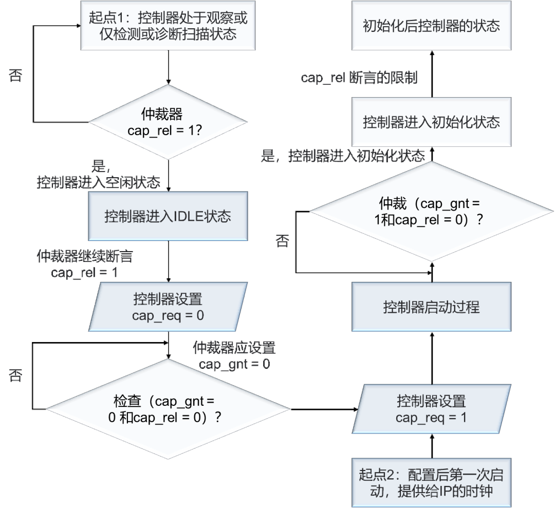
Figure 7. ICAP Arbitration Switching Behavior Flowchart
◾ Debugging Methods
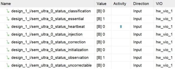
There are mainly two ways to observe the injected error experiments, each with its advantages, to be chosen as needed.
-
Modify the error injection address in the hardware debugging window interface via VIO, then execute the injection trigger.
-
Send commands via serial port, usually recommended to use the simpler serial command method for debugging.
Execute “I” to enter IDLE state
Execute “O” to enter Observation state
Input injection command “N” + “inject_address”;
Execute “S” to obtain the current state, including getting the value of MF (Maximum Frame), ensuring that the injected error does not exceed the boundary. The size of MF varies for different types of devices, such as Virtex-6, 7 series, and Zynq-7000, Ultrascale.
When SEM undergoes state transitions, corresponding print information will be output, starting with “SC”. Error type information starts with “FC”, and can be categorized into four types based on correctable and uncorrectable, necessary and unnecessary errors.
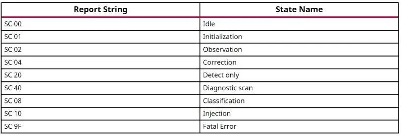
Table 3. Status Report

Table 4. Error Mark Report
◾ Scanning and Error Correction
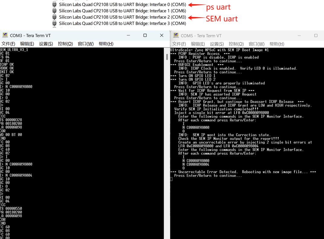
Figure 8. Serial Command Control SEM Scanning and Error Correction
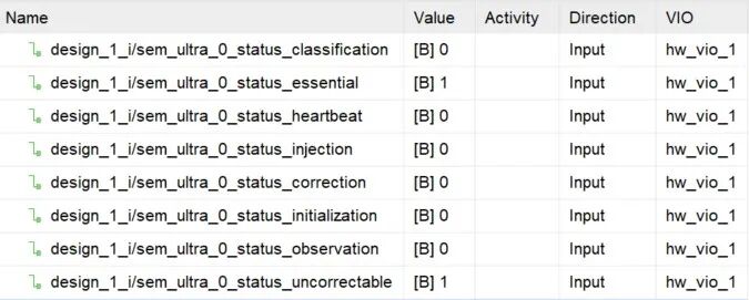
As shown in the figure, through serial commands, the debugging of single-bit and multi-bit error injections was performed, and the SEM scanning and error correction situation was observed. The results were confirmed to be consistent on both sides through VIO monitoring, proving that SEM is functioning correctly.
04
Supplementary Notes on SEM Error Injection
-
Error injection commands will only work if “Error Injection Enable” is checked during IP configuration.
-
Before injection, it must be confirmed to be in IDLE state, and after injection, it must visibly transition to observation to allow the IP to attempt detection or correction.
-
Injecting more than 4 bits at once exceeds the limit (ECC algorithm-based correction that supports correction of configuration memory frames with up to 4-bit errors. See pg187), and the injection command will be lost.
-
Additionally, if the configuration frame does not show changes, it may indicate that the address does not exist.
05
References
❶Integrating LogiCORE SEM IP in Zynq UltraScale+ Devices Application Note (XAPP1298) • Viewer • AMD Technical Information Portal
Scan the QR code below to view
▼▼▼

❷Introduction • UltraScale Architecture Soft Error Mitigation Controller LogiCORE IP Product Guide (PG187) • Reader • AMD Technical Information Portal
Scan the QR code below to view
▼▼▼
END
—— More Exciting Content ——

About Avnet
Avnet is a global leading technology distributor and solutions provider, committed to meeting the evolving needs of customers for over a century. Through a global network of specialized and localized business coverage, Avnet can provide support to customers and suppliers at every stage of the product lifecycle. Avnet helps various types of companies adapt to the changing market environment, accelerating design and supply speed during product development. Avnet is centrally positioned in the entire technology value chain, and this unique position and perspective make it a trusted partner capable of helping customers solve complex design and supply chain challenges, thus achieving revenue faster. For more information about Avnet, please visitwww.avnet.com